ST1280C04K0 Vishay, ST1280C04K0 Datasheet - Page 2
ST1280C04K0
Manufacturer Part Number
ST1280C04K0
Description
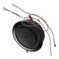
SILICON CONTROLLED RECTIFIER,400V V(DRM),2.3kA I(T),TO-200var48
Manufacturer
Vishay
Specifications of ST1280C04K0
Scr Type
Standard Recovery
Voltage - Off State
400V
Voltage - Gate Trigger (vgt) (max)
3V
Voltage - On State (vtm) (max)
1.44V
Current - On State (it (av)) (max)
2310A
Current - On State (it (rms)) (max)
4150A
Current - Gate Trigger (igt) (max)
200mA
Current - Hold (ih) (max)
600mA
Current - Off State (max)
100mA
Current - Non Rep. Surge 50, 60hz (itsm)
42500A, 44500A
Operating Temperature
-40°C ~ 125°C
Mounting Type
Chassis Mount
Package / Case
TO-200AC, K-PUK, A-24
Current - On State (it (rms) (max)
4150A
Mounting Style
SMD/SMT
Lead Free Status / RoHS Status
Lead free / RoHS Compliant
Other names
*ST1280C04K0
VS-ST1280C04K0
VS-ST1280C04K0
VSST1280C04K0
VSST1280C04K0
VS-ST1280C04K0
VS-ST1280C04K0
VSST1280C04K0
VSST1280C04K0
Available stocks
Company
Part Number
Manufacturer
Quantity
Price
Company:

Part Number:
ST1280C04K0
Manufacturer:
HOLTEK
Quantity:
3 400


ST1280C..K Series
Vishay High Power Products
www.vishay.com
2
ABSOLUTE MAXIMUM RATINGS
PARAMETER
Maximum average on-state current
at heatsink temperature
Maximum RMS on-state current
Maximum peak, one-cycle
non-repetitive surge current
Maximum I
Maximum I
Low level value of threshold voltage
High level value of threshold voltage
Low level value of on-state slope resistance
High level value of on-state slope resistance
Maximum on-state voltage
Maximum holding current
Typical latching current
SWITCHING
PARAMETER
Maximum non-repetitive rate of
rise of turned-on current
Typical delay time
Typical turn-off time
BLOCKING
PARAMETER
Maximum critical rate of rise of
off-state voltage
Maximum peak reverse and
off-state leakage current
2
2
t for fusing
√t for fusing
For technical questions, contact: ind-modules@vishay.com
SYMBOL
SYMBOL
SYMBOL
V
V
I
T(RMS)
dV/dt
I
I
dI/dt
I
I
T(TO)1
T(TO)2
V
RRM
T(AV)
DRM
TSM
Phase Control Thyristors
I
I
r
r
t
t
I
I
2
2
TM
t1
t2
H
d
q
L
(Hockey PUK Version),
t
√t
,
Gate drive 20 V, 20 Ω, t
T
Gate current 1 A, dI
V
I
V
T
T
180° conduction, half sine wave
Double side (single side) cooled
25 °C heatsink temperature double side cooled
t = 10 ms
t = 8.3 ms
t = 10 ms
t = 8.3 ms
t = 10 ms
t = 8.3 ms
t = 10 ms
t = 8.3 ms
t = 0.1 to 10 ms, no voltage reapplied
(16.7 % x π x I
(I > π x I
(16.7 % x π x I
(I > π x I
I
T
TM
pk
J
J
d
R
J
J
2310 A
= T
= 0.67 % V
= T
= T
= 25 °C, anode supply 12 V resistive load
= 8000 A, T
= 50 V, dV/dt = 20 V/µs, gate 0 V 100 Ω, t
= 550 A, T
J
J
J
maximum linear to 80 % rated V
maximum, anode voltage ≤ 80 % V
maximum, rated V
T(AV)
T(AV)
), T
), T
DRM
J
No voltage
reapplied
100 % V
reapplied
No voltage
reapplied
100 % V
reapplied
T(AV)
T(AV)
J
= T
J
J
= T
TEST CONDITIONS
TEST CONDITIONS
TEST CONDITIONS
= T
= T
, T
J
< I < π x I
< I < π x I
g
J
J
maximum, dI/dt = 40 A/µs,
/dt = 1 A/µs
J
J
maximum, t
= 25 °C
maximum
maximum
RRM
RRM
r
≤ 1 µs
DRM
T(AV)
T(AV)
Sinusoidal half wave,
initial T
/V
RRM
p
), T
), T
= 10 ms sine pulse
applied
J
J
J
= T
= T
= T
DRM
J
J
J
DRM
maximum
maximum
maximum
p
= 500 µs
Document Number: 93718
2310 (885)
VALUES
VALUES
VALUES
Revision: 11-Aug-08
55 (85)
42 500
44 500
35 700
37 400
90 270
0.077
0.068
4150
9027
8241
6383
5828
1000
1000
0.83
0.90
1.44
600
200
500
100
1.9
UNITS
UNITS
kA
UNITS
kA
A/µs
V/µs
mΩ
mA
°C
mA
µs
A
A
V
V
2
2
√s
s
Related parts for ST1280C04K0
Image
Part Number
Description
Manufacturer
Datasheet
Request
R

Part Number:
Description:
IR/RF Remote Control Encoder/Decoder IC
Manufacturer:
SunRom
Datasheet:

Part Number:
Description:
357-036-542-201 CARDEDGE 36POS DL .156 BLK LOPRO
Manufacturer:
Vishay
Datasheet:
Part Number:
Description:
357-036-542-201 CARDEDGE 36POS DL .156 BLK LOPRO
Manufacturer:
Vishay
Datasheet:
Part Number:
Description:
357-036-542-201 CARDEDGE 36POS DL .156 BLK LOPRO
Manufacturer:
Vishay
Datasheet:
Part Number:
Description:
357-036-542-201 CARDEDGE 36POS DL .156 BLK LOPRO
Manufacturer:
Vishay
Datasheet:
Part Number:
Description:
357-036-542-201 CARDEDGE 36POS DL .156 BLK LOPRO
Manufacturer:
Vishay
Datasheet:
Part Number:
Description:
357-036-542-201 CARDEDGE 36POS DL .156 BLK LOPRO
Manufacturer:
Vishay
Datasheet:
Part Number:
Description:
357-036-542-201 CARDEDGE 36POS DL .156 BLK LOPRO
Manufacturer:
Vishay
Datasheet:
Part Number:
Description:
357-036-542-201 CARDEDGE 36POS DL .156 BLK LOPRO
Manufacturer:
Vishay
Datasheet:
Part Number:
Description:
357-036-542-201 CARDEDGE 36POS DL .156 BLK LOPRO
Manufacturer:
Vishay
Datasheet:
Part Number:
Description:
357-036-542-201 CARDEDGE 36POS DL .156 BLK LOPRO
Manufacturer:
Vishay
Datasheet:
Part Number:
Description:
357-036-542-201 CARDEDGE 36POS DL .156 BLK LOPRO
Manufacturer:
Vishay
Datasheet:
Part Number:
Description:
357-036-542-201 CARDEDGE 36POS DL .156 BLK LOPRO
Manufacturer:
Vishay
Datasheet:
Part Number:
Description:
357-036-542-201 CARDEDGE 36POS DL .156 BLK LOPRO
Manufacturer:
Vishay
Datasheet:
Part Number:
Description:
357-036-542-201 CARDEDGE 36POS DL .156 BLK LOPRO
Manufacturer:
Vishay
Datasheet: