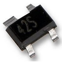
BFP405 Infineon Technologies, BFP405 Datasheet

BFP405
Specifications of BFP405
Available stocks
Related parts for BFP405
BFP405 Summary of contents
Page 1
... For calculation of R please refer to Application Note Thermal Resistance thJA Pin Configuration 1=B 2=E 3=C 4=E Symbol V CEO V CES V CBO V EBO tot stg Symbol R thJS 1 BFP405 Package - - SOT343 Value Unit V 4 150 °C -65 ... 150 -65 ... 150 Value Unit ≤ 520 K/W 2005-10-11 ...
Page 2
... Electrical Characteristics at T Parameter DC Characteristics Collector-emitter breakdown voltage mA Collector-emitter cutoff current Collector-base cutoff current Emitter-base cutoff current current gain mA pulse measured 25°C, unless otherwise specified A Symbol V (BR)CEO I CES I CBO I EBO BFP405 Values Unit min. typ. max. 4 µ 100 µ 130 - 2005-10-11 ...
Page 3
... IP3 value depends on termination of all intermodulation frequency components. Termination used for this measurement is 50 Ω from 0.1 MHz to 6 GHz = 25°C, unless otherwise specified A Symbol Sopt Sopt -1dB = 50 Ω BFP405 Values Unit min. typ. max GHz - 0. dBm - ...
Page 4
... A IKF = 0.16493 - BR = 10.526 mA IKR = 0.25052 Ω 1.9289 V VJE = 0.70367 - XTF = 0.3641 deg PTF = 0 - MJC = 0.48652 fF CJS = 0 - XTB = 0.99469 4 BFP405 1.0405 - NF = 15.761 fA ISE = 0.96647 - NR = 0.037223 fA ISC = 0.21215 mA IRB = 0.12691 Ω 0.37747 - MJE = 0.19762 V VTF = 96.941 fF CJC = 0.08161 - XCJC = 0.75 V VJS = 1. 300 ...
Page 5
... Please note, that the broadest lead is the emitter lead. Common Emitter S- and Noise-parameter For detailed S- and Noise-parameters please contact your local Infineon Technologies distributor or sales office to obtain a Infineon Technologies Application Notes CD-ROM or see Internet: http://www.infineon.com/silicondiscretes EHA07307 5 BFP405 2005-10-11 ...
Page 6
... Permissible Pulse Load = ƒ totmax totDC 0.005 0.01 - 0.02 0.05 0.1 0.2 0 ƒ Permissible Pulse Load K 120 °C 100 150 Collector-base capacitance 1MHz 0.3 pF 0.2 0.15 0.1 0. BFP405 = ƒ thJS p 0.5 0.2 0.1 0.05 0.02 0.01 0.005 ƒ 0.5 1 1 2005-10- ...
Page 7
... I Transition frequency GHz V = parameter GHz ƒ Power gain parameter in GHz Power gain Power gain parameter in GHz 30 GHz 0.9 24 1 BFP405 2 = ƒ Gms Gma |S21|² GHz ƒ 0.5 1 1.5 2 2 2005-10-11 6 0.9 1.8 2 4.5 ...
Page 8
... GHz GHz GHz GHz f = 2.4 GHz 0 1.8 GHz f = 0.9 GHz Source impedance for min. noise figure vs. frequency +j10 0 -j10 4 GHz BFP405 ) Ohm ZS = ZSopt +j50 +j25 +j100 3GHz 4GHz 1.8GHz 5GHz 0.9GHz 6GHz 100 2mA 5mA -j25 -j100 -j50 2005-10-11 ...
Page 9
... Reel ø180 mm = 3.000 Pieces/Reel Reel ø330 mm = 10.000 Pieces/Reel Pin 1 Package SOT343 0.9 ±0.1 2 ±0.2 0.1 MAX. 1 0.15 +0.1 0.6 -0.05 0 0.6 1.15 0.9 Manufacturer Date code (Year/Month) Type code Example 0.2 4 2.15 1.1 9 BFP405 A +0.1 -0.05 2005, June BGA420 2005-10-11 ...
Page 10
... Life support devices or systems are intended to be implanted in the human body support and/or maintain and sustain and/or protect human life. If they fail reasonable to assume that the health of the user or other persons may be endangered. 10 BFP405 2005-10-11 ...


