SI8401DB-T1-E1 Vishay, SI8401DB-T1-E1 Datasheet - Page 7
SI8401DB-T1-E1
Manufacturer Part Number
SI8401DB-T1-E1
Description
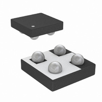
P CH MOSFET, -20V, 4.9A, MICRO FOOT
Manufacturer
Vishay
Series
TrenchFET®r
Specifications of SI8401DB-T1-E1
Transistor Polarity
P Channel
Continuous Drain Current Id
-4.9A
Drain Source Voltage Vds
-20V
On Resistance Rds(on)
95mohm
Rds(on) Test Voltage Vgs
12V
Threshold Voltage Vgs Typ
1.4V
Fet Type
MOSFET P-Channel, Metal Oxide
Fet Feature
Logic Level Gate
Rds On (max) @ Id, Vgs
65 mOhm @ 1A, 4.5V
Drain To Source Voltage (vdss)
20V
Current - Continuous Drain (id) @ 25° C
3.6A
Vgs(th) (max) @ Id
1.4V @ 250µA
Gate Charge (qg) @ Vgs
17nC @ 4.5V
Power - Max
1.47W
Mounting Type
Surface Mount
Package / Case
4-MICRO FOOT®CSP
Lead Free Status / RoHS Status
Lead free / RoHS Compliant
Other names
SI8401DB-T1-E1TR
Available stocks
Company
Part Number
Manufacturer
Quantity
Price

Part Number:
SI8401DB-T1-E1
Manufacturer:
VISHAY/威世
Quantity:
20 000


Á Á Á Á Á Á Á Á Á
Á Á Á Á Á Á Á Á Á
Á Á Á Á Á Á Á Á Á
Á Á Á Á Á Á Á Á Á
Á Á Á Á Á Á Á Á Á
AN824
Vishay Siliconix
MICRO FOOT’S DESIGN AND RELIABILITY
As a mechanical, electrical, and thermal connection between
the device and PCB, the solder bumps of MICRO FOOT
products are mounted on the top active surface of the die.
Table 1 shows the main parameters for solder bumps used in
MICRO FOOT products. A silicon nitride passivation layer is
applied to the active area as the last masking process in
fabrication,ensuring that the device passes the pressure pot
test. A green laser is used to mark the backside of the die
without damaging it. Reliability results for MICRO FOOT
products mounted on a FR-4 board without underfill are shown
in Table 2.
The main failure mechanism associated with wafer-level
chip-scale packaging is fatigue of the solder joint. The results
shown in Table 2 demonstrate that a high level of reliability can
be achieved with proper board design and assembly
techniques.
www.vishay.com
2
Test Condition C: −65_ to 150_C
Test condition B: −40_ to 125_C
121_C @ 15PSI 100% Humidity Test
Á Á Á Á Á Á Á Á Á Á
Á Á Á Á Á Á Á Á Á Á
Á Á Á Á Á Á Á Á Á Á
Á Á Á Á Á Á Á Á Á Á
Á Á Á Á Á Á Á Á Á Á
Á Á Á Á Á Á Á Á Á Á
Á Á Á Á Á Á Á Á Á Á
Á Á Á Á Á Á Á Á Á Á
Á Á Á Á Á Á Á Á Á Á Á Á Á Á Á Á Á Á Á Á Á Á Á Á Á Á Á Á Á Á Á Á
MICRO FOOT CSP MOSFET
MICRO FOOT CSP Analog Switch
MICRO FOOT UCSP Analog Switch
* All measurements in millimeters
MICRO FOOT Reliability Results
MICRO FOOT CSP
Copper
TABLE 2
FIGURE 3. SMD
Solder Mask
Á Á Á Á Á Á Á
Á Á Á Á Á Á Á
Á Á Á Á Á Á Á
Á Á Á Á Á Á Á
Á Á Á Á Á Á Á
Main Parameters of Solder Bumps in MICRO FOOT Designs
Á Á Á Á Á Á
Á Á Á Á Á Á
Á Á Á Á Á Á
Á Á Á Á Á Á
Á Á Á Á Á Á
Á Á Á Á Á Á
Á Á Á Á Á Á
Á Á Á Á Á Á
>1000 Cycles
>500 Cycles
96 Hours
Bump Material
Eutectic Solder:
Eutectic Solder:
63Sm/37Pb
63Sm/37Pb
Á Á Á Á Á Á Á
Á Á Á Á Á Á Á
Á Á Á Á Á Á Á
Á Á Á Á Á Á Á
Á Á Á Á Á Á Á
Á Á Á Á Á Á Á
Á Á Á Á Á Á Á
Á Á Á Á Á Á Á
TABLE 1
Bump Pitch*
BOARD LAYOUT GUIDELINES
Board materials. Vishay Siliconix MICRO FOOT products are
designed to be reliable on most board types, including organic
boards such as FR-4 or polyamide boards. The package
qualification information is based on the test on 0.5-oz. FR-4
and polyamide boards with NSMD pad design.
Land patterns. Two types of land patterns are used for
surface-mount packages. Solder mask defined (SMD) pads
have a solder mask opening smaller than the metal pad
(Figure 3), whereas on-solder mask defined (NSMD) pads
have a metal pad smaller than the solder-mask opening
(Figure 4).
NSMD is recommended for copper etch processes, since it
provides a higher level of control compared to SMD etch
processes. A small-size NSMD pad definition provides more
area (both lateral and vertical) for soldering and more room for
escape routing on the PCB. By contrast, SMD pad definition
introduces a stress concentration point near the solder mask
on the PCB side that may result in solder joint cracking under
extreme fatigue conditions.
Copper pads should be finished with an organic solderability
preservative
nickel-immersion gold finish pads, the gold thickness must be
less than 0.5 mm to avoid solder joint embrittlement.
0.8
0.5
0.5
Á Á Á Á Á Á
Á Á Á Á Á Á
Á Á Á Á Á Á
Á Á Á Á Á Á
Á Á Á Á Á Á
Á Á Á Á Á Á
Á Á Á Á Á Á
Á Á Á Á Á Á
Bump Diameter*
(OSP)
Copper
0.37-0.41
0.18-0.25
0.32-0.34
FIGURE 4. NSMD
coating.
Solder Mask
Á Á Á Á Á Á Á
Á Á Á Á Á Á Á
Á Á Á Á Á Á Á
Á Á Á Á Á Á Á
Á Á Á Á Á Á Á
Á Á Á Á Á Á Á
Á Á Á Á Á Á Á
Á Á Á Á Á Á Á
Bump Height*
Document Number: 71990
For
0.26-0.29
0.14-0.19
0.21-0.24
electroplated
06-Jan-03
Related parts for SI8401DB-T1-E1
Image
Part Number
Description
Manufacturer
Datasheet
Request
R


Part Number:
Description:
P-Channel 20-V (D-S) MOSFET
Manufacturer:
VISHAY [Vishay Siliconix]
Datasheet:

Part Number:
Description:
P-channel 20-v D-s Mosfet
Manufacturer:
Vishay
Datasheet:

Part Number:
Description:
357-036-542-201 CARDEDGE 36POS DL .156 BLK LOPRO
Manufacturer:
Vishay
Datasheet:
Part Number:
Description:
357-036-542-201 CARDEDGE 36POS DL .156 BLK LOPRO
Manufacturer:
Vishay
Datasheet:
Part Number:
Description:
357-036-542-201 CARDEDGE 36POS DL .156 BLK LOPRO
Manufacturer:
Vishay
Datasheet:
Part Number:
Description:
357-036-542-201 CARDEDGE 36POS DL .156 BLK LOPRO
Manufacturer:
Vishay
Datasheet:
Part Number:
Description:
357-036-542-201 CARDEDGE 36POS DL .156 BLK LOPRO
Manufacturer:
Vishay
Datasheet:
Part Number:
Description:
357-036-542-201 CARDEDGE 36POS DL .156 BLK LOPRO
Manufacturer:
Vishay
Datasheet:
Part Number:
Description:
357-036-542-201 CARDEDGE 36POS DL .156 BLK LOPRO
Manufacturer:
Vishay
Datasheet:
Part Number:
Description:
357-036-542-201 CARDEDGE 36POS DL .156 BLK LOPRO
Manufacturer:
Vishay
Datasheet:
Part Number:
Description:
357-036-542-201 CARDEDGE 36POS DL .156 BLK LOPRO
Manufacturer:
Vishay
Datasheet:
Part Number:
Description:
357-036-542-201 CARDEDGE 36POS DL .156 BLK LOPRO
Manufacturer:
Vishay
Datasheet: