SIA431DJ-T1-GE3 Vishay, SIA431DJ-T1-GE3 Datasheet
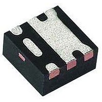
P CHANNEL MOSFET, -20V, 12A

SIA431DJ-T1-GE3

Manufacturer Part Number
SIA431DJ-T1-GE3
Description
P CHANNEL MOSFET, -20V, 12A
Manufacturer
Vishay
Datasheet

Specifications of SIA431DJ-T1-GE3

Transistor Polarity
P Channel
Continuous Drain Current Id
-12A
Drain Source Voltage Vds
-20V
On Resistance Rds(on)
25mohm
Rds(on) Test Voltage Vgs
-4.5V
Threshold Voltage Vgs Typ
-850mV
Configuration
Single
Resistance Drain-source Rds (on)
0.07 Ohms
Forward Transconductance Gfs (max / Min)
31 S
Drain-source Breakdown Voltage
- 20 V
Continuous Drain Current
- 12 A
Power Dissipation
19 W
Maximum Operating Temperature
+ 150 C
Mounting Style
SMD/SMT
Package / Case
PowerPAK SC-70-6L
Gate Charge Qg
60 nC
Minimum Operating Temperature
- 55 C
Lead Free Status / RoHS Status
Lead free / RoHS Compliant

Available stocks

Company
Part Number
Manufacturer
Quantity
Price
Part Number:
SIA431DJ-T1-GE3
Manufacturer:
VISHAY
Quantity:
3 000
Part Number:
SIA431DJ-T1-GE3
Manufacturer:
VISHAY/威世
Quantity:
20 000
Company:
Part Number:
SIA431DJ-T1-GE3
Quantity:
714
Company:
Part Number:
SIA431DJ-T1-GE3
Quantity:
526
Company:
Part Number:
SIA431DJ-T1-GE3
Quantity:
2 609
Notes:
a. Package limited.
b. Surface mounted on 1" x 1" FR4 board.
c. t = 5 s.
d. See Solder Profile (www.vishay.com/ppg?73257). The PowerPAK SC-70 is a leadless package. The end of the lead terminal is exposed
e. Rework conditions: manual soldering with a soldering iron is not recommended for leadless components.
f. Maximum under Steady State conditions is 80 °C/W.
Document Number: 65267
S09-1536-Rev. A, 10-Aug-09
PRODUCT SUMMARY
ABSOLUTE MAXIMUM RATINGS T
Parameter
Drain-Source Voltage
Gate-Source Voltage
Continuous Drain Current (T
Pulsed Drain Current
Continuous Source-Drain Diode Current
Maximum Power Dissipation
Operating Junction and Storage Temperature Range
Soldering Recommendations (Peak Temperature)
THERMAL RESISTANCE RATINGS
Parameter
Maximum Junction-to-Ambient
Maximum Junction-to-Case (Drain)
V
copper (not plated) as a result of the singulation process in manufacturing. A solder fillet at the exposed copper tip cannot be guaranteed and
is not required to ensure adequate bottom side solder interconnection.
DS
- 20
2.05 mm
6
(V)
PowerPAK SC-70-6L-Single
D
5
D
4
0.025 at V
0.031 at V
0.041 at V
0.070 at V
S
D
R
1
S
DS(on)
D
2.05 mm
2
GS
GS
GS
GS
G
= - 4.5 V
= - 2.5 V
= - 1.8 V
= - 1.5 V
(Ω)
J
3
= 150 °C)
b, f
P-Channel 20-V (D-S) MOSFET
Ordering Information: SiA431DJ-T1-GE3 (Lead (Pb)-free and Halogen-free)
Part # code
I
- 12
- 12
- 12
D
- 4
(A)
a
a
a
d, e
A
Marking Code
= 25 °C, unless otherwise noted
Q
Steady State
g
24 nC
T
T
T
T
T
T
T
T
T
T
(Typ.)
B K X
X X X
C
C
A
A
C
A
C
C
A
A
t ≤ 5 s
= 25 °C
= 70 °C
= 25 °C
= 70 °C
= 25 °C
= 25 °C
= 25 °C
= 70 °C
= 25 °C
= 70 °C
Lot traceability
and Date code
FEATURES
APPLICATIONS
• Halogen-free According to IEC 61249-2-21
• TrenchFET
• New Thermally Enhanced PowerPAK
• 100 % R
• Compliant to RoHS Directive 2002/95/EC
• Load Switch, PA Switch and Battery Switch for Portable
Symbol
Symbol
T
R
R
Definition
SC-70 Package
- Small Footprint Area
- Low On-Resistance
Devices
J
V
V
I
thJA
thJC
P
, T
DM
I
I
GS
DS
D
S
D
stg
g
Tested
®
Power MOSFET
Typical
5.3
28
- 55 to 150
- 9.6
- 7.7
- 2.9
Limit
3.5
2.2
- 12
- 12
- 12
- 20
- 30
260
± 8
19
12
b, c
b, c
b, c
b, c
b, c
a
a
a
Maximum
6.5
36
Vishay Siliconix
G
P-Channel MOSFET
®
SiA431DJ
www.vishay.com
S
D
°C/W
Unit
Unit
°C
W
V
A
1

Related parts for SIA431DJ-T1-GE3

SIA431DJ-T1-GE3 Summary of contents

Page 1

... 2. 2. Ordering Information: SiA431DJ-T1-GE3 (Lead (Pb)-free and Halogen-free) ABSOLUTE MAXIMUM RATINGS T Parameter Drain-Source Voltage Gate-Source Voltage Continuous Drain Current (T = 150 °C) J Pulsed Drain Current Continuous Source-Drain Diode Current Maximum Power Dissipation Operating Junction and Storage Temperature Range Soldering Recommendations (Peak Temperature) ...

Page 2

... SiA431DJ Vishay Siliconix SPECIFICATIONS °C, unless otherwise noted J Parameter Static Drain-Source Breakdown Voltage V Temperature Coefficient DS V Temperature Coefficient GS(th) Gate-Source Threshold Voltage Gate-Source Leakage Zero Gate Voltage Drain Current a On-State Drain Current a Drain-Source On-State Resistance a Forward Transconductance b Dynamic Input Capacitance Output Capacitance ...

Page 3

... 2000 1500 1000 500 1.5 1.4 1.3 1.2 1 1.0 0.9 0.8 0 SiA431DJ Vishay Siliconix ° 125 ° °C C 0.0 0.3 0.6 0.9 1 Gate-to-Source Voltage (V) GS Transfer Characteristics C iss C oss C rss Drain-to-Source Voltage (V) DS Capacitance 4.5 V and 2 ...

Page 4

... SiA431DJ Vishay Siliconix TYPICAL CHARACTERISTICS 25 °C, unless otherwise noted 100 150 ° 0.1 0.0 0.2 0.4 0.6 0 Source-to-Drain Voltage (V) SD Soure-Drain Diode Forward Voltage 0.9 0.8 0 250 µA D 0.6 0.5 0.4 0.3 0 Temperature (°C) J Threshold Voltage www.vishay.com 4 0.08 0.06 0. °C 0.02 ...

Page 5

... It is used to determine the current rating, when this rating falls below the package limit. Document Number: 65267 S09-1536-Rev. A, 10-Aug- 100 125 150 = 150 °C, using junction-to-case thermal resistance, and is more useful in settling the upper SiA431DJ Vishay Siliconix 100 125 T - Case Temperature (°C) C Power Derating www.vishay.com 150 ...

Page 6

... SiA431DJ Vishay Siliconix TYPICAL CHARACTERISTICS 25 °C, unless otherwise noted 1 Duty Cycle = 0.5 0.2 0.1 0.05 0.02 Single Pulse 0. Normalized Thermal Transient Impedance, Junction-to-Ambient 1 Duty Cycle = 0.5 0.2 0.1 0.05 0.02 Single Pulse 0 Vishay Siliconix maintains worldwide manufacturing capability. Products may be manufactured at one of several qualified locations. Reliability data for Silicon Technology and Package Reliability represent a composite of all qualified locations ...

Page 7

... Vishay disclaims any and all liability arising out of the use or application of any product described herein or of any information provided herein to the maximum extent permitted by law. The product specifications do not expand or otherwise modify Vishay’ ...

Related keywords