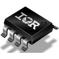
IRF7220PBF International Rectifier, IRF7220PBF Datasheet - Page 2

IRF7220PBF
Manufacturer Part Number
IRF7220PBF
Description
P CHANNEL MOSFET, -14V, 11A, SOIC
Manufacturer
International Rectifier
Specifications of IRF7220PBF
Transistor Polarity
P Channel
Continuous Drain Current Id
11A
Drain Source Voltage Vds
-14V
On Resistance Rds(on)
12mohm
Rds(on) Test Voltage Vgs
-4.5V
Threshold Voltage Vgs Typ
-600mV
Channel Type
P
Current, Drain
±11 A
Gate Charge, Total
84 nC
Package Type
SO-8
Polarization
P-Channel
Power Dissipation
2.5 W
Resistance, Drain To Source On
0.0082 Ohm
Temperature, Operating, Maximum
+150 °C
Temperature, Operating, Minimum
-55 °C
Time, Turn-off Delay
140 ns
Time, Turn-on Delay
19 ns
Transconductance, Forward
8.4 S
Voltage, Breakdown, Drain To Source
-14 V
Voltage, Drain To Source
–12 V
Voltage, Forward, Diode
-1.2 V
Voltage, Gate To Source
±12 V
Configuration
Single Quad Drain Triple Source
Resistance Drain-source Rds (on)
12 mOhms
Drain-source Breakdown Voltage
- 12 V
Gate-source Breakdown Voltage
12 V
Continuous Drain Current
- 11 A
Maximum Operating Temperature
+ 150 C
Mounting Style
SMD/SMT
Package / Case
SOIC-8
Fall Time
1040 ns
Gate Charge Qg
84 nC
Minimum Operating Temperature
- 55 C
Rise Time
420 ns
Lead Free Status / RoHS Status
Lead free / RoHS Compliant
Lead Free Status / RoHS Status
Lead free / RoHS Compliant
Available stocks
Company
Part Number
Manufacturer
Quantity
Price
Part Number:
IRF7220PBF
Manufacturer:
IR
Quantity:
20 000
‚
IRF7220
Source-Drain Ratings and Characteristics
Notes:
Electrical Characteristics @ T
I
I
V
t
Q
SM
S
rr
V
V
g
Q
Q
Q
t
t
t
t
C
C
C
R
I
d(on)
d(off)
2
I
r
f
SD
DSS
rr
Repetitive rating; pulse width limited by
V
Pulse width
fs
(BR)DSS
GS(th)
GSS
iss
oss
rss
max. junction temperature.
g
gs
gd
DS(on)
(BR)DSS
/ T
J
Continuous Source Current
(Body Diode)
Pulsed Source Current
(Body Diode)
Diode Forward Voltage
Reverse Recovery Time
Reverse RecoveryCharge
Drain-to-Source Breakdown Voltage
Breakdown Voltage Temp. Coefficient
Gate Threshold Voltage
Forward Transconductance
Gate-to-Source Forward Leakage
Gate-to-Source Reverse Leakage
Total Gate Charge
Gate-to-Source Charge
Gate-to-Drain ("Miller") Charge
Turn-On Delay Time
Rise Time
Turn-Off Delay Time
Fall Time
Input Capacitance
Output Capacitance
Reverse Transfer Capacitance
Static Drain-to-Source On-Resistance
Drain-to-Source Leakage Current
300µs; duty cycle
Parameter
Parameter
2%.
J
= 25°C (unless otherwise specified)
ƒ
„
When mounted on 1 inch square copper board, t<10 sec
R
Starting T
Min. Typ. Max. Units
–––
–––
–––
–––
–––
-0.60 –––
G
Min. Typ. Max. Units
––– -0.006 –––
––– .0082 0.012
––– .0125 0.020
–––
–––
–––
–––
–––
–––
–––
–––
–––
–––
––– 1040 –––
––– 8075 –––
––– 4400 –––
––– 4150 –––
-14
8.4
= 25 , I
–––
160
147
–––
–––
–––
–––
––– -100
––– -100
–––
420
140
–––
84
13
37
19
J
= 25°C, L = 1.8mH
AS
-1.2
220
240
= 11A. (See Figure 10)
-88
-2.5
-5.0
–––
–––
–––
125
–––
–––
–––
100
20
55
V/°C
nC
ns
µA
V
nA
nC
ns
pF
A
V
S
V
p-n junction diode.
di/dt = 100A/µs
MOSFET symbol
showing the
integral reverse
T
T
V
Reference to 25°C, I
V
V
V
V
V
V
V
V
I
V
V
V
I
R
R
V
V
ƒ = 1.0MHz
J
J
D
D
GS
GS
GS
DS
DS
DS
DS
GS
GS
DS
GS
DD
GS
DS
G
D
= 25°C, I
= 25°C, I
= -11A
= -11A
= 0.91 ‚
= 6.2
= 0V, I
= -4.5V, I
= -2.5V, I
= V
= -10V, I
= -11.2V, V
= -11.2V, V
= -12V
= 12V
= -10V
= -5.0V ‚
= -10V
= 0V
= -10V
GS
Conditions
, I
D
S
F
Conditions
D
= -5mA
= -2.5A
= -2.5A, V
D
D
D
= -250µA
‚
= -11A
= -11A ‚
= -8.8A ‚
GS
GS
= 0V
= 0V, T
www.irf.com
D
= -1mA
GS
G
= 0V ‚
J
= 70°C
D
S


