J304-E3 Vishay, J304-E3 Datasheet - Page 5
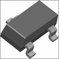
J304-E3
Manufacturer Part Number
J304-E3
Description
N CHANNEL JFET, -40V, TO-92
Manufacturer
Vishay
Datasheet
1.J305-E3.pdf
(7 pages)
Specifications of J304-E3
Breakdown Voltage Vbr
-40V
Gate-source Cutoff Voltage Vgs(off) Max
-1.5V
Power Dissipation Pd
350mW
Operating Temperature Range
-55°C To +150°C
No. Of Pins
3
Continuous Drain Current Id
1mA
Channel Type
N
Configuration
Single
Gate-source Voltage (max)
-30V
Drain-gate Voltage (max)
-30V
Operating Temperature (min)
-55C
Operating Temperature (max)
150C
Operating Temperature Classification
Military
Mounting
Through Hole
Pin Count
3
Package Type
TO-92
Lead Free Status / RoHS Status
Lead free / RoHS Compliant


TYPICAL CHARACTERISTICS (T
Document Number: 70236
S-50077—Rev. E, 24-Jan-05
0.01
100
0.1
0.1
10
10
5
4
3
2
1
0
1
1
100
100
0
T
V
V
Common Source
T
V
V
Common Source
f = 1 MHz
A
A
DS
GS
DS
GS
= 25_C
= 25_C
Common-Source Input Capacitance
= 15 V
= 15 V
= 0 V
= 0 V
−4
V
vs. Gate-Source Voltage
GS
200
200
V
Reverse Admittance
f − Frequency (MHz)
DS
− Gate-Source Voltage (V)
Input Admittance
f − Frequency (MHz)
= 0 V
−8
V
DS
= 10 V
−12
500
500
−b
b
−16
is
rs
A
−g
g
= 25_C UNLESS OTHERWISE NOTED)
is
rs
1000
1000
−20
Common-Source Reverse Feedback Capacitance
0.01
2.4
1.8
1.2
0.6
100
0.1
0.1
10
10
3
0
1
1
100
100
0
T
V
V
Common Source
A
DS
GS
f = 1 MHz
= 25_C
= 15 V
= 0 V
vs. Gate-Source Voltage
−4
V
g
fs
DS
V
GS
= 0 V
200
200
Forward Admittance
Output Admittance
f − Frequency (MHz)
− Gate-Source Voltage (V)
f − Frequency (MHz)
−8
V
DS
Vishay Siliconix
= 10 V
−b
fs
b
T
V
V
Common Source
−12
os
A
DS
GS
= 25_C
= 15 V
= 0 V
J304/305
500
500
www.vishay.com
g
−16
os
1000
1000
−20
5
Related parts for J304-E3
Image
Part Number
Description
Manufacturer
Datasheet
Request
R


Part Number:
Description:
357-036-542-201 CARDEDGE 36POS DL .156 BLK LOPRO
Manufacturer:
Vishay
Datasheet:
Part Number:
Description:
357-036-542-201 CARDEDGE 36POS DL .156 BLK LOPRO
Manufacturer:
Vishay
Datasheet:
Part Number:
Description:
357-036-542-201 CARDEDGE 36POS DL .156 BLK LOPRO
Manufacturer:
Vishay
Datasheet:
Part Number:
Description:
357-036-542-201 CARDEDGE 36POS DL .156 BLK LOPRO
Manufacturer:
Vishay
Datasheet:
Part Number:
Description:
357-036-542-201 CARDEDGE 36POS DL .156 BLK LOPRO
Manufacturer:
Vishay
Datasheet:
Part Number:
Description:
357-036-542-201 CARDEDGE 36POS DL .156 BLK LOPRO
Manufacturer:
Vishay
Datasheet:
Part Number:
Description:
357-036-542-201 CARDEDGE 36POS DL .156 BLK LOPRO
Manufacturer:
Vishay
Datasheet:
Part Number:
Description:
357-036-542-201 CARDEDGE 36POS DL .156 BLK LOPRO
Manufacturer:
Vishay
Datasheet:
Part Number:
Description:
357-036-542-201 CARDEDGE 36POS DL .156 BLK LOPRO
Manufacturer:
Vishay
Datasheet:
Part Number:
Description:
357-036-542-201 CARDEDGE 36POS DL .156 BLK LOPRO
Manufacturer:
Vishay
Datasheet:
Part Number:
Description:
357-036-542-201 CARDEDGE 36POS DL .156 BLK LOPRO
Manufacturer:
Vishay
Datasheet:
Part Number:
Description:
357-036-542-201 CARDEDGE 36POS DL .156 BLK LOPRO
Manufacturer:
Vishay
Datasheet: