2N5114-E3 Vishay, 2N5114-E3 Datasheet
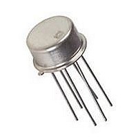
P CHANNEL JFET, 45V, TO-206AA

2N5114-E3

Manufacturer Part Number
2N5114-E3
Description
P CHANNEL JFET, 45V, TO-206AA
Manufacturer
Vishay
Datasheets

Specifications of 2N5114-E3

Breakdown Voltage Vbr
45V
Gate-source Cutoff Voltage Vgs(off) Max
10V
Power Dissipation Pd
500mW
Operating Temperature Range
-55°C To +200°C
No. Of Pins
3
Transistor Polarity
P Channel
Channel Type
P
Configuration
Single
Gate-source Voltage (max)
30V
Drain-gate Voltage (max)
30V
Operating Temperature (min)
-55C
Operating Temperature Classification
Military
Mounting
Through Hole
Pin Count
3
Continuous Drain Current Id
-90mA
Rohs Compliant
Yes
Lead Free Status / RoHS Status
Lead free / RoHS Compliant
DESCRIPTION
The 2N4338/4339/4340/4341 n-channel JFETs are designed
for sensitive amplifier stages at low- to mid-frequencies. Low
cut-off voltages accommodate low-level power supplies and
low leakage for improved system accuracy.
ABSOLUTE MAXIMUM RATINGS
Gate-Source/Gate-Drain Voltage
Forward Gate Current
Storage Temperature
Operating Junction Temperature
For applications information see AN102 and AN106.
Document Number: 70240
S-40990—Rev. F, 24-May-04
PRODUCT SUMMARY
FEATURES
D Low Cutoff Voltage: 2N4338 <1 V
D High Input Impedance
D Very Low Noise
D High Gain: A
Part Number
2N4338
2N4339
2N4340
2N4341
V
. . . . . . . . . . . . . . . . . . . . . . . . . . . . . . . . . . . . . . . . .
. . . . . . . . . . . . . . . . . . . . . . . . . . . . . . . . . . .
V
= 80 @ 20 mA
−0.6 to −1.8
GS(off)
−0.3 to −1
−1 to −3
−2 to −6
. . . . . . . . . . . . . . . . . . . . . . . . . .
. . . . . . . . . . . . . . . . . . . . . . . . . . . . . . .
(V)
V
(BR)GSS
−50
−50
−50
−50
Min (V)
BENEFITS
D Full Performance from Low-Voltage
D Low Signal Loss/System Error
D High System Sensitivity
D High-Quality Low-Level Signal
Power Supply: Down to 1 V
Amplification
N-Channel JFETs
−65 to 200_C
−55 to 175_C
D
S
g
50 mA
fs
−50 V
1
2
Min (mS)
TO-206AA
0.6
0.8
1.3
Top View
(TO-18)
2
The TO-206AA (TO-18) package is hermetically sealed and
suitable for military processing (see Military Information). For
similar products in TO-226AA (TO-92) and TO-236 (SOT-23)
packages, see the J/SST201 series data sheet.
Lead Temperature (
Power Dissipation
Notes
a.
3
I
DSS
Derate 2 mW/_C above 25_C
G and Case
Max (mA)
0.6
1.5
3.6
9
a
1
. . . . . . . . . . . . . . . . . . . . . . . . . . . . . . . . . . . . . . . . .
/
2N4338/4339/4340/4341
16
” from case for 10 sec.)
APPLICATIONS
D High-Gain, Low-Noise Amplifiers
D Low-Current, Low-Voltage
D Infrared Detector Amplifiers
D Ultrahigh Input Impedance
Battery-Powered Amplifiers
Pre-Amplifiers
Vishay Siliconix
. . . . . . . . . . . . . . . . . . .
www.vishay.com
300 mW
300_C
1

Related parts for 2N5114-E3

2N5114-E3 Summary of contents

Page 1

... G and Case Top View −50 V Lead Temperature ( Power Dissipation 50 mA −65 to 200_C Notes −55 to 175_C a. Derate 2 mW/_C above 25_C 2N4338/4339/4340/4341 Vishay Siliconix APPLICATIONS D High-Gain, Low-Noise Amplifiers D Low-Current, Low-Voltage Battery-Powered Amplifiers D Infrared Detector Amplifiers D Ultrahigh Input Impedance Pre-Amplifiers 1 / ” from case for 10 sec ...

Page 2

... Vishay Siliconix SPECIFICATIONS FOR 2N4338 AND 2N4339 (T Parameter Symbol Static Gate-Source Breakdown Voltage V Gate-Source Cutoff Voltage V b Saturation Drain Current Gate Reverse Current Gate Reverse Current b Gate Operating Current Drain Cutoff Current c Gate-Source Forward Voltage Dynamic Common-Source Forward Transconductance Common-Source ...

Page 3

... MHz = MHz rss kHz kHz 25_C UNLESS OTHERWISE NOTED 100 0 −4 −5 0 2N4338/4339/4340/4341 Vishay Siliconix Limits 2N4340 2N4341 a Typ Min Max Min 1 1500 Gate Leakage Current I = 100 mA D 500 125_C 125_C GSS 500 100 25_C 25_C GSS − Drain-Gate Voltage (V) ...

Page 4

... Vishay Siliconix TYPICAL CHARACTERISTICS (T On-Resistance and Output Conductance vs. Gate-Source Cutoff Voltage 1500 g os 1200 900 r DS 600 300 100 mA kHz −1 −2 V − Gate-Source Cutoff Voltage (V) GS(off) Output Characteristics 400 V = −0.7 V GS(off) 320 240 160 80 −0 − Drain-Source Voltage (V) DS ...

Page 5

... Transconductance vs. Gate-Source Voltage kHz 3.2 2.4 1.6 0 −0.4 −0.5 2000 1600 1200 800 = −0 400 0 1 0.01 2N4338/4339/4340/4341 Vishay Siliconix Transfer Characteristics = −1 GS(off −55_C A 25_C 125_C −0.4 −0.8 −1.2 −1.6 V − Gate-Source Voltage ( −1 GS(off kHz T = −55_C A 25_C 125_C − ...

Page 6

... Vishay Siliconix TYPICAL CHARACTERISTICS (T Common-Source Input Capacitance vs. Gate-Source Voltage MHz −4 −8 −12 V − Gate-Source Voltage (V) GS Output Conductance vs. Drain Current −1.5 V GS(off) 2.4 1.8 T 0.8 25_C 0.4 0 0.01 0.1 I − Drain Current (mA) D www.vishay.com 6 = 25_C UNLESS OTHERWISE NOTED −16 − ...

Page 7

... Vishay disclaims any and all liability arising out of the use or application of any product described herein or of any information provided herein to the maximum extent permitted by law. The product specifications do not expand or otherwise modify Vishay’ ...

Related keywords