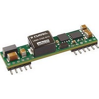
LSN2-T/10-D12G-C Murata Power Solutions Inc, LSN2-T/10-D12G-C Datasheet - Page 13

LSN2-T/10-D12G-C
Manufacturer Part Number
LSN2-T/10-D12G-C
Description
DC/DC Converter
Manufacturer
Murata Power Solutions Inc
Series
LSN2r
Datasheet
1.LSN2-T10-D12G-C.pdf
(15 pages)
Specifications of LSN2-T/10-D12G-C
No. Of Outputs
1
Input Voltage
8.3V To 14V
Power Rating
50W
Output Current
10A
Approval Bodies
UL, CSA
Supply Voltage
14VDC
Dc / Dc Converter Case Style
SIP
Dc/dc Converter Mounting
Through Hole
Product
Non-Isolated / POL
Output Power
50 W
Input Voltage Range
8.3 V to 14 V
Input Voltage (nominal)
12 V
Number Of Outputs
1
Output Voltage (channel 1)
0.75 V to 5 V
Output Current (channel 1)
10 A
Package / Case Size
SIP
Output Type
Low Voltage Selectable
Output Voltage
0.75 V to 5 V
Lead Free Status / RoHS Status
Lead free / RoHS Compliant
[6] Allow the converter to eventually achieve its full-rated setpoint output
[7] The Sequence is a sensitive input into the feedback control loop of the
[8] If one converter is slaving to another master converter, there will be a very
[9] You may connect two or more Sequence inputs in parallel from two
[10] Any external capacitance added to the converter’s output may affect
Notice in the simplifi ed Sequence/Track equivalent circuit (Figure 15) that
a blocking diode effectively disconnects this circuit when the Sequence/
Track pin is pulled up to +V
voltage. Do not remain in ramp up/down mode indefi nitely. The converter
is characterized and meets all its specifi cations only at the setpoint
voltage (plus or minus any trim voltage). During the ramp-up phase, the
converter is not considered fully in regulation. This may affect perfor-
mance with excessive high current loads at turn-on.
converter. Avoid noise and long leads on this input. Keep all wiring very
short. Use shielding if necessary. Consider adding a small parallel ce-
ramic capacitor across the Sequence/Track input (see Figure 14) to block
any external high frequency noise.
short phase lag between the two converters. This can usually be ignored.
converters. Be aware of the increasing pull-up bias current and reduced
input impedance.
ramp up/down times and ramp tracking accuracy.
Figure 15. Sequence/Track Simplifi ed Equivalent Schematic
IN
or left open.
www.murata-ps.com
Power Good Output
The Power Good Output consists of an unterminated BSS138 small signal
fi eld effect transistor and a dual window comparator input circuit driving the
gate of the FET. Power Good is TRUE (open drain, high impedance state) if the
converter’s power output voltage is within about ±10% of the setpoint. Thus,
the PG TRUE condition indicates that the converter is approximately within
regulation. Since an overcurrent condition occurs at about 2% output voltage
reduction, the Power Good does not directly measure an output overcurrent
condition at rated maximum output current. However, gross overcurrent or
an output short circuit will set Power Good to FALSE (+0.2V saturation, low
impedance condition).
Common connection), the Power Good output is unterminated so that the user
may adapt the output to a variety of logic families. The PG pin may therefore
be used with logic voltages which are not necessarily the same as the input
or output power voltages. Install an external pullup resistor to the logic supply
voltage which is compatible with your logic system. When the Power Good is
out of limit, the FET is at saturation, approximately +0.2V output. Keep this
LOW (FALSE) pulldown current to less than 10mA.
Ignore Power Good while in transition.
Using a simple connection to external logic (and returned to the converter’s
Please note that Power Good is briefl y false during Sequence ramp-up.
Figure 16. Equivalent Power Good Circuit
Selectable-Output DC/DC Converters
25 Jun 2010
Non-isolated, DOSA-SIP, 6/10/16A
LSN2 Series
MDC_LSN2.B07Δ
email: sales@murata-ps.com
Page 13 of 15


