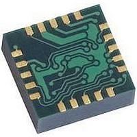
HMC5843 Honeywell Microelectronics & Precision Sensors, HMC5843 Datasheet - Page 20

HMC5843
Manufacturer Part Number
HMC5843
Description
Magnetic Sensor
Manufacturer
Honeywell Microelectronics & Precision Sensors
Datasheet
1.HMC5843.pdf
(21 pages)
Specifications of HMC5843
Msl
MSL 3 - 168 Hours
Sensitivity Range
+/- 10 %
Sensor Terminals
PCB
Magnetic Field Max
4G
Axis Configuration
Three
Sensor Output
Digital
Available stocks
Company
Part Number
Manufacturer
Quantity
Price
Company:
Part Number:
HMC5843
Manufacturer:
HITTITE
Quantity:
3 000
Company:
Part Number:
HMC5843-DEMO
Manufacturer:
Honeywell Microelectronics & P
Quantity:
135
Company:
Part Number:
HMC5843-EVAL
Manufacturer:
Honeywell Microelectronics & P
Quantity:
135
HMC5843
Identification Register B
The identification register B is used to identify the device. IRB0 through IRB7 indicate bit locations, with IRB denoting the
bits that are in the identification register A. IRB7 denotes the first bit of the data stream.
Register values. ASCII value 4
Identification Register C
The identification register C is used to identify the device. IRC0 through IRC7 indicate bit locations, with IRC denoting the
bits that are in the identification register A. IRC7 denotes the first bit of the data stream.
Register values. ASCII value 3
I
The HMC5843 communicates via a two-wire I2C bus system as a slave device. The HMC5843 uses a simple protocol
with the interface protocol defined by the I2C bus specification, and by this document. The data rate is at the standard-
mode 100kbps or 400kbps rates as defined in the I2C Bus Specifications. The bus bit format is an 8 -bit Data/Address
send and a 1 -bit acknowledge bit. The format of the data bytes (payload) shall be case sensitive ASCII characters or
binary data to the HMC5843 slave, and binary data returned. Negative binary values will be in two’s complement form.
The default (factory) HMC5843 7-bit slave address is 0x3C for write operations, or 0x3D for read operations.
The HMC5843 Serial Clock (SCL) and Serial Data (SDA) lines have optional internal pull-up resistors, but require resistive
pull-ups (Rp) between the master device (usually a host microprocessor) and the HMC5843. Pull-up resistance values of
about 10k ohms are recommended with a nominal 1.8-volt digital supply voltage (DVDD). Other values may be used as
defined in the I2C Bus Specifications or with the internal 50k ohm pull-up resistors (SDAP, SCLP) that can be tied to
DVDD.
The SCL and SDA lines in this bus specification can be connected to a host of devices. The bus can be a single master to
multiple slaves, or it can be a multiple master configuration. All data transfers are initiated by the master device which is
responsible for generating the clock signal, and the data transfers are 8 bit long. All devices are addressed by I2C’s
unique 7 bit address. After each 8-bit transfer, the master device generates a 9 th clock pulse, and releases the SDA line.
The receiving device (addressed slave) will pull the SDA line low to acknowledge (ACK) the successful transfer or leave
the SDA high to negative acknowledge (NACK).
Per the I2C spec, all transitions in the SDA line must occur when SCL is low. This requirement leads to two unique
conditions on the bus associated with the SDA transitions when SCL is high. Master device pulling the SDA line low while
the SCL line is high indicates the Start (S) condition, and the Stop (P) condition is when the SDA line is pulled high while
the SCL line is high. The I2C protocol also allows for the Restart condition in which the master device issues a second
start condition without issuing a stop.
All bus transactions begin with the master device issuing the start sequence followed by the slave address byte. The
address byte contains the slave address; the upper 7 bits (bits7-1), and the Least Significant bit (LSb). The LSb of the
address byte designates if the operation is a read (LSb=1) or a write (LSb=0). At the 9 th clock pulse, the recieving slave
device will issue the ACK (or NACK). Following these bus events, the master will send data bytes for a write operation, or
the slave will clock out data with a read operation. All bus transactions are terminated with the master issuing a stop
sequence.
20
2
C COMMUNICATION PROTOCOL
IRB7
0
IRC7
0
IRB6
0
IRC6
0
Table 24: Identification Register C Default Values
Table 23: Identification Register B Default Values
IRC5
1
IRB5
1
IRB4
1
IRC4
1
IRB3
0
IRC3
0
IRB2
1
IRC2
0
IRB1
0
IRC1
1
IRB0
0
IRC0
1
www.honeywell.com


