TLE4916-1K Infineon Technologies, TLE4916-1K Datasheet
TLE4916-1K
Specifications of TLE4916-1K
Available stocks


Related parts for TLE4916-1K

TLE4916-1K Summary of contents
Page 1
... TLE4916- Rev.1.0, 2010-02- & ...
Page 2
... Infineon Technologies Office. Infineon Technologies components may be used in life-support devices or systems only with the express written approval of Infineon Technologies failure of such components can reasonably be expected to cause the failure of that life-support device or system or to affect the safety or effectiveness of that device or system. Life support devices or systems are intended to be implanted in the human body or to support and/or maintain and sustain and/or protect human life ...
Page 3
... TLE4916-1K Low-Power Automotive Hall Switch Revision History: 2010-02-23, Rev.1.0 Previous Version: Page Subjects (major changes since last revision) We Listen to Your Comments Any information within this document that you feel is wrong, unclear or missing at all? Your feedback will help us to continuously improve the quality of this document. ...
Page 4
... Functional Block Description 5 3 Specification 7 3.1 Application Circuit 7 3.2 Absolute Maximum Ratings 8 3.3 Operating Range 8 3.4 Electrical and Magnetic Characteristics 9 4 Package Information 11 4.1 Package Outline SC59 11 4.2 Footprint 12 4.3 Distance between Chip and Package 13 4.4 Package Marking 13 Datasheet 2 TLE4916-1K Table of Contents Rev.1.0, 2010-02-23 ...
Page 5
... Target Applications Target applications for TLE4916-1K are all automotive and industrial applications which require a low-power Hall switch to save power consumption. Due to its low average supply current of typical 4µA the sensor is ideally suited for battery powered systems or applications with a stand-by mode. ...
Page 6
... Pin Configuration (top view 1.5 ± 0.15 SC59 Figure 1 Pin Configuration and Center of Sensitive Area 2.3 Pin Description Table 1 Pin Description Pin No. Symbol GND Datasheet QSAT Center of Sensitive Area ± 0.15 0.8 Function Supply voltage Output Ground 4 TLE4916-1K Functional Description Comment Rev.1.0, 2010-02-23 ...
Page 7
... Functional Block Diagram 2.5 Functional Block Description The TLE4916- integrated Hall-Effect Sensor designed specifically to meet the requirements of low-power applications with operating voltages of 2.4V - 5.0V. Precise magnetic switching points and high temperature stability are achieved through the unique design of the internal circuit. ...
Page 8
... I Operating S Time I SOPAVG I SAVG I SSTB Figure 3 Timing Diagram Figure 4 Output Signal Datasheet Standby Time stb μ 70ms TLE4916-1K Functional Description Latch t Output B Rev.1.0, 2010-02-23 ...
Page 9
... For operating the sensor a pull-up resistor is required. A ceramic bypass capacitor GND is recommended. Note: The size of the pull-up resistor increases the overall current consumption as additional current is flowing through this resistor. C Figure 5 Application Circuit Datasheet Vs = 100nF S GND 7 TLE4916-1K Specification R = 5kΩ Rev.1.0, 2010-02-23 ...
Page 10
... Human Body Model (HBM) tests according to: EOS/ESD Association Standard S5.1-1993 and Mil. Std. 883D method 3015.7 3.3 Operating Range The following operating conditions must not be exceeded in order to ensure correct operation of the TLE4916-1K. All parameters specified in the following sections refer to these operating conditions unless otherwise mentioned. Table 4 Operating Condition Parameters ...
Page 11
... QSAT I – 0.01 QLEAK t – 0 – 0 – 70 stb – – 0.07 op stb SOPAVG 9 TLE4916-1K unless other conditions are stated. Unit Note / Test Condition Max. ≤ 10 µA V 3.3V s ≤ ≤ -40°C T 125°C j ≤ 5.0V s ≤ ≤ -40°C T 85°C j ≤ 5.0V s ≤ ...
Page 12
... Positive magnetic fields are defined with the south pole of the magnet to the branded side of package Branded Side Figure 6 Definition of magnetic field direction Datasheet 1) Symbol Values Min. Typ 3 -3 HYS T – -700 C 10 TLE4916-1K Unit Note / Test Condition Max – ppm/° 2.7V and T = 25° Rev.1.0, 2010-02-23 Specification ...
Page 13
... Package Information 4.1 Package Outline SC59 3 ±0.1 3x0.4 1 0.95 Figure 7 SC59 Package Outline (All dimensions in mm) Datasheet +0.05 -0.1 0 0.95 (0.55) 11 TLE4916-1K Package Information 1.1 ±0.1 0.15 MAX. 0.1 +0.1 0.2 0˚...8˚ MAX. GPS09473 Rev.1.0, 2010-02-23 ...
Page 14
... Footprint 0.8 1.2 0.8 Reflow Soldering Figure 8 Footprint SC59 Datasheet 0.8 1.2 0.8 Wave Soldering 12 TLE4916-1K Package Information Rev.1.0, 2010-02-23 ...
Page 15
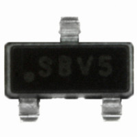
... Distance between Chip and Package Branded Side d: Distance chip to upper side 0.56 ±0.1 Figure 9 Distance between chip and package 4.4 Package Marking Year (y) = 0...9 Month (m) = 1... Figure 10 Marking of TLE4916-1K Datasheet October n - November d - December 13 TLE4916-1K Package Information Rev.1.0, 2010-02-23 ...
Page 16
... Published by Infineon Technologies AG ...