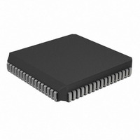
PIC16LC924-04/L Microchip Technology, PIC16LC924-04/L Datasheet - Page 89

PIC16LC924-04/L
Manufacturer Part Number
PIC16LC924-04/L
Description
IC,MICROCONTROLLER,8-BIT,PIC CPU,CMOS,LDCC,68PIN,PLASTIC
Manufacturer
Microchip Technology
Series
PIC® 16Cr
Specifications of PIC16LC924-04/L
Rohs Compliant
YES
Core Processor
PIC
Core Size
8-Bit
Speed
4MHz
Connectivity
I²C, SPI
Peripherals
LCD, POR, PWM, WDT
Number Of I /o
25
Program Memory Size
7KB (4K x 14)
Program Memory Type
OTP
Ram Size
176 x 8
Voltage - Supply (vcc/vdd)
2.5 V ~ 6 V
Data Converters
A/D 5x8b
Oscillator Type
External
Operating Temperature
0°C ~ 70°C
Package / Case
68-PLCC
Processor Series
PIC16LC
Core
PIC
Data Bus Width
8 bit
Data Ram Size
176 B
Interface Type
I2C, SPI
Maximum Clock Frequency
8 MHz
Number Of Programmable I/os
25
Number Of Timers
3
Operating Supply Voltage
2.5 V to 6 V
Maximum Operating Temperature
+ 70 C
Mounting Style
SMD/SMT
3rd Party Development Tools
52715-96, 52716-328, 52717-734
Development Tools By Supplier
ICE2000
Minimum Operating Temperature
0 C
On-chip Adc
8 bit, 5 Channel
Lead Free Status / RoHS Status
Lead free / RoHS Compliant
Eeprom Size
-
Lead Free Status / Rohs Status
Details
Other names
PIC16LC924-04/LR
PIC16LC924-04/LR
PIC16LC924-04/LR
Available stocks
Company
Part Number
Manufacturer
Quantity
Price
Company:
Part Number:
PIC16LC924-04/L
Manufacturer:
Microchip Technology
Quantity:
10 000
13.0
The LCD module generates the timing control to drive
a static or multiplexed LCD panel, with support for up to
32 segments multiplexed with up to 4 commons. It also
provides control of the LCD pixel data.
The interface to the module consists of 3 control regis-
ters (LCDCON, LCDSE, and LCDPS) used to define
the timing requirements of the LCD panel and up to 16
LCD data registers (LCD00-LCD15) that represent the
array of the pixel data. In normal operation, the control
registers are configured to match the LCD panel being
used. Primarily, the initialization information consists of
selecting the number of commons required by the LCD
panel, and then specifying the LCD Frame clock rate to
be used by the panel.
FIGURE 13-1: LCDCON REGISTER (ADDRESS 10Fh)
1997 Microchip Technology Inc.
bit7
bit 7:
bit 6:
bit 5:
bit 4:
bit 3-2: CS1:CS0: Clock Source Select bits
bit 1-0: LMUX1:LMUX0: Common Selection bits
LCDEN
R/W-0
LMUX1:LMUX0
LCD MODULE
00
01
10
11
LCDEN: Module drive enable bit
1 = LCD drive enabled
0 = LCD drive disabled
SLPEN: LCD display sleep enable
1 = LCD module will stop operating during SLEEP
0 = LCD module will continue to display during SLEEP
Unimplemented: Read as '0'
VGEN: Voltage Generator Enable
1 = Internal LCD Voltage Generator Enabled, (powered-up)
0 = Internal LCD Voltage Generator powered-down, voltage is expected to be provided externally
00 = Fosc/256
01 = T1CKI (Timer1)
1x = Internal RC oscillator
Specifies the number of commons and the bias method
SLPEN
R/W-0
U-0
—
MULTIPLEX
Static (COM0)
1/2
1/3
1/4
VGEN
R/W-0
(COM0, 1)
(COM0, 1, 2)
(COM0, 1, 2, 3)
R/W-0
CS1
BIAS
Static
1/3
1/3
1/3
R/W-0
CS0
Once the module is initialized for the LCD panel, the
individual bits of the LCD data registers are cleared/set
to represent a clear/dark pixel respectively.
Once
(LCDCON<7>) bit is used to enable or disable the LCD
module. The LCD panel can also operate during sleep
by clearing the SLPEN (LCDCON<6>) bit.
Figure 13-4 through Figure 13-7 provides waveforms
for Static, 1/2, 1/3, and 1/4 MUX drives.
Max # of Segments
LMUX1
R/W-0
the
32
31
30
29
bit0
LMUX0
R/W-0
module
R =Readable bit
W =Writable bit
U =Unimplemented bit,
Read as ‘0’
-n =Value at POR reset
is
PIC16C9XX
configured,
DS30444E - page 89
the
LCDEN


