PIC16LC923-04I/L Microchip Technology, PIC16LC923-04I/L Datasheet - Page 43
PIC16LC923-04I/L
Manufacturer Part Number
PIC16LC923-04I/L
Description
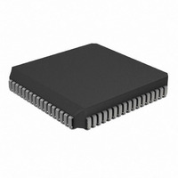
IC,MICROCONTROLLER,8-BIT,PIC CPU,CMOS,LDCC,68PIN,PLASTIC
Manufacturer
Microchip Technology
Series
PIC® 16Cr
Datasheet
1.PIC16C923-04L.pdf
(189 pages)
Specifications of PIC16LC923-04I/L
Rohs Compliant
YES
Core Processor
PIC
Core Size
8-Bit
Speed
4MHz
Connectivity
I²C, SPI
Peripherals
LCD, POR, PWM, WDT
Number Of I /o
25
Program Memory Size
7KB (4K x 14)
Program Memory Type
OTP
Ram Size
176 x 8
Voltage - Supply (vcc/vdd)
2.5 V ~ 6 V
Oscillator Type
External
Operating Temperature
-40°C ~ 85°C
Package / Case
68-PLCC
Processor Series
PIC16LC
Core
PIC
Data Bus Width
8 bit
Data Ram Size
176 B
Interface Type
I2C, SPI
Maximum Clock Frequency
8 MHz
Number Of Programmable I/os
25
Number Of Timers
3
Operating Supply Voltage
2.5 V to 6 V
Maximum Operating Temperature
+ 85 C
Mounting Style
SMD/SMT
3rd Party Development Tools
52715-96, 52716-328, 52717-734
Development Tools By Supplier
ICE2000
Minimum Operating Temperature
- 40 C
Lead Free Status / RoHS Status
Lead free / RoHS Compliant
Eeprom Size
-
Data Converters
-
Lead Free Status / Rohs Status
Details
Available stocks
Company
Part Number
Manufacturer
Quantity
Price
Company:

Part Number:
PIC16LC923-04I/L
Manufacturer:
Microchip Technology
Quantity:
10 000


6.0
Each module can generate an interrupt to indicate that
an event has occurred (e.g. timer overflow). Each of
these modules is explained in full detail in the following
sections. The timer modules are:
• Timer0 Module (Section 7.0)
• Timer1 Module (Section 8.0)
• Timer2 Module (Section 9.0)
6.1
The Timer0 module is a simple 8-bit timer/counter. The
clock source can be either the internal system clock
(Fosc/4) or an external clock. When the clock source is
an external clock, the Timer0 module can be selected
to increment on either the rising or falling edge.
The Timer0 module also has a programmable prescaler
option. This prescaler can be assigned to either the
Timer0 module or the Watchdog Timer. Bit PSA
(OPTION<3>) assigns the prescaler, and bits PS2:PS0
(OPTION<2:0>) determine the prescaler value. Timer0
can increment at the following rates: 1:1 when pres-
caler assigned to Watchdog timer, 1:2, 1:4, 1:8, 1:16,
1:32, 1:64, 1:128, and 1:256.
Synchronization of the external clock occurs after the
prescaler. When the prescaler is used, the external
clock frequency may be higher then the device’s fre-
quency. The maximum frequency is 50 MHz, given the
high and low time requirements of the clock.
6.2
Timer1 is a 16-bit timer/counter. The clock source can
be either the internal system clock (Fosc/4), an external
clock, or an external crystal. Timer1 can operate as
either a timer or a counter. When operating as a counter
(external clock source), the counter can either operate
synchronized to the device or asynchronously to the
device. Asynchronous operation allows Timer1 to oper-
ate during sleep, which is useful for applications that
require a real-time clock as well as the power savings
of SLEEP mode.
Timer1 also has a prescaler option which allows Timer1
to increment at the following rates: 1:1, 1:2, 1:4, and
1:8. Timer1 can be used in conjunction with the Cap-
ture/Compare/PWM module. When used with a CCP
module, Timer1 is the time-base for 16-bit capture or
the 16-bit compare and must be synchronized to the
device. Timer1 oscillator is also one of the clock
sources for the LCD module.
6.3
Timer2 is an 8-bit timer with a programmable prescaler
and postscaler, as well as an 8-bit period register
(PR2). Timer2 can be used with the CCP1 module (in
PWM mode) as well as the clock source for the Syn-
1997 Microchip Technology Inc.
OVERVIEW OF TIMER
MODULES
Timer0 Overview
Timer1 Overview
Timer2 Overview
chronous Serial Port (SSP). The prescaler option
allows Timer2 to increment at the following rates: 1:1,
1:4, 1:16.
The postscaler allows the TMR2 register to match the
period register (PR2) a programmable number of times
before generating an interrupt. The postscaler can be
programmed from 1:1 to 1:16 (inclusive).
6.4
The CCP module can operate in one of these three
modes: 16-bit capture, 16-bit compare, or up to 10-bit
Pulse Width Modulation (PWM).
Capture mode captures the 16-bit value of TMR1 into
the CCPR1H:CCPR1L register pair. The capture event
can be programmed for either the falling edge, rising
edge, fourth rising edge, or the sixteenth rising edge of
the CCP1 pin.
Compare mode compares the TMR1H:TMR1L register
pair to the CCPR1H:CCPR1L register pair. When a
match occurs an interrupt can be generated, and the
output pin CCP1 can be forced to given state (High or
Low), TMR1 can be reset and start A/D conversion.
This depends on the control bits CCP1M3:CCP1M0.
PWM mode compares the TMR2 register to a 10-bit
duty cycle register (CCPR1H:CCPR1L<5:4>) as well
as to an 8-bit period register (PR2). When the TMR2
register = Duty Cycle register, the CCP1 pin will be
forced low. When TMR2 = PR2, TMR2 is cleared to 00h,
an interrupt can be generated, and the CCP1 pin (if an
output) will be forced high.
CCP Overview
PIC16C9XX
DS30444E - page 43
Related parts for PIC16LC923-04I/L
Image
Part Number
Description
Manufacturer
Datasheet
Request
R

Part Number:
Description:
IC MCU OTP 4KX14 LCD DVR 64TQFP
Manufacturer:
Microchip Technology
Datasheet:

Part Number:
Description:
IC MCU OTP 4KX14 LCD DVR 68PLCC
Manufacturer:
Microchip Technology
Datasheet:
Part Number:
Description:
IC MCU OTP 4KX14 LCD DVR 64TQFP
Manufacturer:
Microchip Technology
Datasheet:

Part Number:
Description:
IC MCU 64 LD LOW 64-SDIP
Manufacturer:
Microchip Technology
Datasheet:
Part Number:
Description:
IC MCU 64 LD LOW 64-SDIP
Manufacturer:
Microchip Technology
Datasheet:

Part Number:
Description:
Manufacturer:
Microchip Technology Inc.
Datasheet:
Part Number:
Description:
Manufacturer:
Microchip Technology Inc.
Datasheet:
Part Number:
Description:
Manufacturer:
Microchip Technology Inc.
Datasheet:
Part Number:
Description:
Manufacturer:
Microchip Technology Inc.
Datasheet:
Part Number:
Description:
Manufacturer:
Microchip Technology Inc.
Datasheet:
Part Number:
Description:
Manufacturer:
Microchip Technology Inc.
Datasheet: