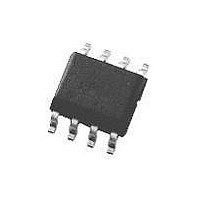
LP3982IMM-1.8 National Semiconductor, LP3982IMM-1.8 Datasheet - Page 8

LP3982IMM-1.8
Manufacturer Part Number
LP3982IMM-1.8
Description
Linear Voltage Regulator IC
Manufacturer
National Semiconductor
Datasheets
1.LP3982IMMX-2.82.pdf
(12 pages)
2.LP3982IMM-2.5.pdf
(12 pages)
3.LP3982IMM-2.5.pdf
(12 pages)
Specifications of LP3982IMM-1.8
Dropout Voltage Vdo
120mV
No. Of Pins
8
Output Current
0.3A
Operating Temperature Range
-40°C To +85°C
Linear Regulator Type
LDO Fixed Positive
Mounting Type
Surface Mount
Lead Free Status / RoHS Status
Contains lead / RoHS non-compliant
Available stocks
Company
Part Number
Manufacturer
Quantity
Price
Company:
Part Number:
LP3982IMM-1.8
Manufacturer:
NS
Quantity:
23
Company:
Part Number:
LP3982IMM-1.8
Manufacturer:
NS
Quantity:
195
Part Number:
LP3982IMM-1.8
Manufacturer:
NS/国半
Quantity:
20 000
Part Number:
LP3982IMM-1.8/NOPB
Manufacturer:
NS/国半
Quantity:
20 000
www.national.com
Application Information
The LP3982 generates an internal zero that makes up for the
inadequately high zero of the low ESR ceramic output ca-
pacitor. This internally generated zero is strategically placed
to provide positive phase shift near unity gain, thus providing
a stable phase margin.
NO-LOAD STABILITY
The LP3982 remains stable during no-load conditions, a
necessary feature for CMOS RAM keep-alive applications.
INPUT CAPACITOR
The LP3982 requires a minimum input capacitance of about
1µF. The value may be increased indefinitely. The type is not
critical to stability. However, instability may occur with bench
set-ups where long supply leads are used, particularly at
near dropout and high current conditions. This is attributed to
the lead inductance coupling to the output through the gate
oxide of the pass transistor; thus, forming a pseudo LCR
network within the Loop-gain. A 10µF tantalum input capaci-
tor remedies this non-situ condition; its larger ESR acts to
dampen the pseudo LCR network. This may only be neces-
sary for some bench setups. 1µF ceramic input capacitor are
fine for most end-use applications.
If a tantalum input capacitor is intended for the final applica-
tion, it is important to consider their tendency to fail in short
circuit mode, thus potentially damaging the part.
NOISE BYPASS CAPACITOR
The noise bypass capacitor (CC) significantly reduces output
noise of the LP3982. It connects between pin 6 and ground.
The optimum value for CC is 33nF.
Pin 6 directly connects to the high impedance output of the
bandgap. The DC leakage of the CC capacitor should be
considered; loading down the reference will reduce the out-
put voltage. NPO and COG ceramic capacitors typically offer
very low leakage. Polypropylene and polycarbonate film car-
bonate capacitor offer even lower leakage currents.
CC does not affect the transient response; however, it does
affect turn-on time. The smaller the CC value, the quicker the
turn-on time.
Inadequately High Zero for Stability Compensation
FIGURE 4. Loop Gain Bode Plot Illustrating
(Continued)
20036919
8
POWER DISSIPATION
Power dissipation refers to the part’s ability to radiate heat
away from the silicon, with packaging being a key factor. A
reasonable analogy is the packaging a human being might
wear, a jacket for example. A jacket keeps a person comfort-
able on a cold day, but not so comfortable on a hot day. It
would be even worse if the person was exerting power
(exercising). This is because the jacket has resistance to
heat flow to the outside ambient air, like the IC package has
a thermal resistance from its junctions to the ambient (θ
θ
calculate the IC’s junction temperature as follows:
T
resistance from the junction to the ambient air outside the
package. PD is the power exerted by the IC, and T
ambient temperature.
PD is calculated as follows:
θ
forced air flow, 182˚C/W with 225 linear feet per minute
(LFPM) of air flow, 163˚C/W with 500 LFPM of air flow, and
149˚C/W with 900 LFPM of air flow.
θ
layout of the PC board: heavy traces (particularly at V
the two V
Improvements and absolute measurements of the θ
be estimated by utilizing the thermal shutdown circuitry that
is internal to the IC. The thermal shutdown turns off the pass
transistor of the device when its junction temperature
reaches 160˚C (Typical). The pass transistor doesn’t turn on
again until the junction temperature drops about 10˚C (hys-
teresis).
Using the thermal shutdown circuit to estimate , θ
done as follows: With a low input to output voltage differen-
tial, set the load current to 300mA. Increase the input voltage
until the thermal shutdown begins to cycle on and off. Then
slowly decrease V
on. Record the resulting voltage differential (V
the following equation:
FAULT DETECTION
The LP3982 provides a FAULT pin that goes low during out
of regulation conditions like current limit and thermal shut-
down, or when it approaches dropout. The latter monitors
the input-to-output voltage differential and compares it
against a threshold that is slightly above the dropout voltage.
This threshold also tracks the dropout voltage as it varies
with load current. Refer to Fault Detect vs. Load Current
curve in the typical characteristics section.
The FAULT pin requires a pull-up resistor since it is an
open-drain output. This resistor should be large in value to
reduce energy drain. A 100kΩ pull-up resistor works well for
most applications.
Figure 5 shows the LP3985 with delay added to the FAULT
pin for the reset pin of a microprocessor. The output of the
comparator stays low for a preset amount of time after the
regulator comes out of a fault condition.
JA
JA
JA
J
is the junction temperature of the IC. θ
has a unit of temperature per power and can be used to
for the LP3982 package (MSOP-8) is 223˚C/W with no
can also be decreased (improved) by considering the
OUT
pins), large planes, through-holes, etc.
IN
PD = I
T
(100mV increments) until the part stays
J
= θ
OUT
JA
(PD) + T
(V
IN
-V
O
A
)
JA
D
is the thermal
) and use it in
JA
A
can be
JA
IN
is the
and
JA
can
).


