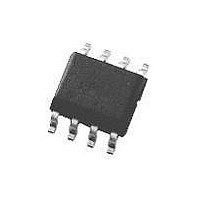
LP3982IMM-1.8 National Semiconductor, LP3982IMM-1.8 Datasheet - Page 7

LP3982IMM-1.8
Manufacturer Part Number
LP3982IMM-1.8
Description
Linear Voltage Regulator IC
Manufacturer
National Semiconductor
Datasheets
1.LP3982IMMX-2.82.pdf
(12 pages)
2.LP3982IMM-2.5.pdf
(12 pages)
3.LP3982IMM-2.5.pdf
(12 pages)
Specifications of LP3982IMM-1.8
Dropout Voltage Vdo
120mV
No. Of Pins
8
Output Current
0.3A
Operating Temperature Range
-40°C To +85°C
Linear Regulator Type
LDO Fixed Positive
Mounting Type
Surface Mount
Lead Free Status / RoHS Status
Contains lead / RoHS non-compliant
Available stocks
Company
Part Number
Manufacturer
Quantity
Price
Company:
Part Number:
LP3982IMM-1.8
Manufacturer:
NS
Quantity:
23
Company:
Part Number:
LP3982IMM-1.8
Manufacturer:
NS
Quantity:
195
Part Number:
LP3982IMM-1.8
Manufacturer:
NS/国半
Quantity:
20 000
Part Number:
LP3982IMM-1.8/NOPB
Manufacturer:
NS/国半
Quantity:
20 000
Application Information
Similarity in the output capabilities exists between op amps
and linear regulators. Just as rail-to-rail output op amps
allow their output voltage to approach the supply voltage,
low dropout regulators (LDOs) allow their output voltage to
operate close to the input voltage. Both achieve this by the
configuration of their output transistors. Standard op amps
and regulator outputs are at the source (or emitter) of the
output transistor. Rail-to-rail op amp and LDO regulator out-
puts are at the drain (or collector) of the output transistor.
This replaces the threshold (or diode drop) limitations on the
output with the less restrictive source-to-drain (or V
tations. There is a trade-off, of course. The output imped-
ance become significantly higher, thus providing a critically
lower pole when combined with the capacitive load. That’s
why rail-to-rail op amps are usually poor at driving capacitive
loads and recommend a series output resistor when doing
so. LDOs require the same series resistance except that the
internal resistance of the output capacitor will usually suffice.
Refer to the output capacitance section for more information.
OUTPUT CAPACITANCE
The LP3982 is specifically designed to employ ceramic out-
put capacitors as low as 2.2µF. Ceramic capacitors below
10µF offer significant cost and space savings, along with
high frequency noise filtering. Higher values and other types
and of capacitor may be used, but their equivalent series
resistance (ESR) should be maintained below 0.5Ω
Ceramic capacitor of the value required by the LP3982 are
available in the following dielectric types: Z5U, Y5V, X5R and
X7R. The Z5U and Y5V types exhibit a 50% or more drop in
capacitance value as their temperature increases from 25˚C,
an important consideration. The X5R generally maintain their
capacitance value within
for their tighter tolerance of 10% over temperature.
Ceramic capacitors pose a challenge because of their rela-
tively low ESR. Like most other LDOs, the LP3982 relies on
a zero in the frequency response to compensate against
excessive phase shift in the regulator’s feedback loop. If the
phase shift reaches 360˚ (i.e.; becomes positive), the regu-
lator will oscillate. This compensation usually resides in the
zero generated by the combination of the output capacitor
with its equivalent series resistance (ESR). The zero is
intended to cancel the effects of the pole generated by the
load capacitance (C
tion of the load resistance (R
(R
capacitors is that the zero it generates can be too high in
frequency for the pole that it’s intended to compensate. The
LP3982 overcomes this challenge by internally generating a
strategically placed zero.
O
) of the regulator. The challenge posed by low ESR
L
) combined with the parallel combina-
±
20%. The X7R type are desirable
L
) and the output resistance
(Continued)
SAT
) limi-
7
Figure 3 shows a basic model for the linear regulator that
helps describe what happens to the output signal as it is
processed through its feedback loop; that is, describe its
loop gain (LG). The LG includes two main transfer functions:
the error amplifier and the load. The error amplifier provides
voltage gain and a dominant pole, while the load provides a
zero and a pole. The LG of the model in Figure 3 is described
by the following equation:
The first term of the above equation expresses the voltage
gain (numerator) and a single pole role-off (denominator) of
the error amplifier. The second term expresses the zero
(numerator) and pole (denominator) of the load in combina-
tion with the R
Figure 4 shows a Bode plot that represents a case where the
zero contributed by the load is too high to cancel the effect of
the pole contributed by the load and R
illustrates the loop gain while the dashed line illustrates the
corresponding phase shift. Notice that the phase shift at
unity gain is a total 360˚ -the criteria for oscillation.
FIGURE 3. Simplified Model of Regulator
O
of the regulator.
Loop Gain Components
O
. The solid line
www.national.com
20036917


