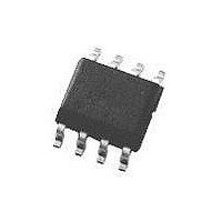
LP2987IMM-3.3 National Semiconductor, LP2987IMM-3.3 Datasheet - Page 7

LP2987IMM-3.3
Manufacturer Part Number
LP2987IMM-3.3
Description
Linear Voltage Regulator IC
Manufacturer
National Semiconductor
Datasheets
1.LP2988AIMM-3.3.pdf
(23 pages)
2.LP2988AIMM-3.3.pdf
(24 pages)
3.LP2988AIMM-3.3.pdf
(19 pages)
Specifications of LP2987IMM-3.3
Primary Input Voltage
16V
Dropout Voltage Vdo
180mV
No. Of Pins
8
Output Current
200mA
Operating Temperature Range
-40°C To +125°C
Termination Type
SMD
Mounting Type
Surface Mount
Lead Free Status / RoHS Status
Contains lead / RoHS non-compliant
Available stocks
Company
Part Number
Manufacturer
Quantity
Price
Company:
Part Number:
LP2987IMM-3.3
Manufacturer:
NS
Quantity:
3
Company:
Part Number:
LP2987IMM-3.3
Manufacturer:
NSC
Quantity:
30 000
Company:
Part Number:
LP2987IMM-3.3
Manufacturer:
NS
Quantity:
30 000
Part Number:
LP2987IMM-3.3
Manufacturer:
NS/国半
Quantity:
20 000
I
SHUTDOWN INPUT
V
I
ERROR COMPARATOR
I
V
V
(MAX)
V
(MIN)
HYST
DELAY
S/D
OH
Limits in standard typeface are for T
less otherwise specified: V
S/D
OL
THR
THR
Electrical Characteristics
Note 1: Absolute Maximum Ratings indicate limits beyond which damage to the component may occur. Electrical specifications do not apply when operating the de-
vice outside of its rated operating conditions.
Note 2: The ESD rating of the Bypass pin is 500V (LP2988 only.)
Note 3: The maximum allowable power dissipation is a function of the maximum junction temperature, T
and the ambient temperature, T
The value of
excessive die temperature, and the regulator will go into thermal shutdown.
Note 4: If used in a dual-supply system where the regulator load is returned to a negative supply, the LM2987/8 output must be diode-clamped to ground.
Note 5: The output PNP structure contains a diode between the V
on this diode and may induce a latch-up mode which can damage the part (see Application Hints).
Note 6: Limits are 100% production tested at 25˚C. Limits over the operating temperature range are guaranteed through correlation using Statistical Quality Control
(SQC) methods. The limits are used to calculate National’s Average Outgoing Quality Level (AOQL).
Note 7: Dropout voltage is defined as the input to output differential at which the output voltage drops 100 mV below the value measured with a 1V differential.
Note 8: To prevent mis-operation, the Shutdown input must be driven by a signal that swings above V
Application Hints).
Note 9: Temperature coefficient is defined as the maximum (worst-case) change divided by the total temperature range.
Note 10: See Typical Performance Characteristics curves.
Symbol
J−A
Delay Pin Current
Source
S/D Input Voltage
(Note 8)
S/D Input Current
Output “HIGH” Leakage
Output “LOW” Voltage
Upper Threshold
Voltage
Lower Threshold
Voltage
Hysteresis
for the SO-8 (M) package is 160˚C/W, and the mini SO-8 (MM) package is 200˚C/W. Exceeding the maximum allowable power dissipation will cause
Parameter
A
. The maximum allowable power dissipation at any ambient temperature is calculated using:
IN
= V
O
(NOM) + 1V, I
J
= 25˚C, and limits in boldface type apply over the full operating temperature range. Un-
V
V
V
V
V
V
I
O
H
L
S/D
S/D
OH
IN
(COMP) = 300 µA
(Continued)
= O/P OFF
= O/P ON
= V
= 16V
= 0
= 5V
Conditions
L
O
(NOM) − 0.5V,
= 1 mA, C
IN
and V
OUT
OUT
terminals that is normally reverse-biased. Forcing the output above the input will turn
7
= 4.7 µF, C
Typical
−4.6
−6.6
0.55
0.01
150
2.2
1.4
2.0
0
5
IN
= 2.2 µF, V
LM2987/8AI-X.X
−13.0
−5.5
−7.7
−8.9
H
Min
1.6
1.4
1.6
and below V
J
(MAX), the junction-to-ambient thermal resistance,
(Note 6)
S/D
−2.5
Max
0.18
−3.5
−4.9
−3.3
220
350
2.8
3.0
L
−1
15
1
2
with a slew rate not less than 40 mV/µs (see
= 2V.
−13.0
LM2987/8I-X.X
−7.7
−5.5
−8.9
Min
1.6
1.4
1.6
(Note 6)
Max
0.18
−3.5
−2.5
−4.9
−3.3
220
350
2.8
3.0
−1
15
1
2
www.national.com
%V
Units
mV
µA
µA
µA
V
J−A
OUT
,


