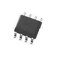
LP2987IMM-3.3 National Semiconductor, LP2987IMM-3.3 Datasheet - Page 16

LP2987IMM-3.3
Manufacturer Part Number
LP2987IMM-3.3
Description
Linear Voltage Regulator IC
Manufacturer
National Semiconductor
Datasheets
1.LP2988AIMM-3.3.pdf
(23 pages)
2.LP2988AIMM-3.3.pdf
(24 pages)
3.LP2988AIMM-3.3.pdf
(19 pages)
Specifications of LP2987IMM-3.3
Primary Input Voltage
16V
Dropout Voltage Vdo
180mV
No. Of Pins
8
Output Current
200mA
Operating Temperature Range
-40°C To +125°C
Termination Type
SMD
Mounting Type
Surface Mount
Lead Free Status / RoHS Status
Contains lead / RoHS non-compliant
Available stocks
Company
Part Number
Manufacturer
Quantity
Price
Company:
Part Number:
LP2987IMM-3.3
Manufacturer:
NS
Quantity:
3
Company:
Part Number:
LP2987IMM-3.3
Manufacturer:
NSC
Quantity:
30 000
Company:
Part Number:
LP2987IMM-3.3
Manufacturer:
NS
Quantity:
30 000
Part Number:
LP2987IMM-3.3
Manufacturer:
NS/国半
Quantity:
20 000
www.national.com
Application Hints
The external capacitor c
The value of capacitor required for a given time delay may
be calculated using the formula:
To simplify design, a plot is provided below which shows val-
ues of C
DETAILS OF ERR/RESET CIRCUIT OPERATION: (Refer
to LP2987/8 Equivalent Circuit).
DLY
versus delay time.
Timing Diagram for Power-Up
C
DLY
Plot of C
= T
DELAY
DLY
DLY
sets the delay time (T
(Continued)
/(5.59 X 10
vs T
DELAY
5
DS100017-11
)
DS100017-9
DELAY
).
16
The output of comparator U2 is the ERR/RESET flag. Since
it is an open-collector output, it requires the use of a pull-up
resistor (R
put of U2, which means that its output is controlled by the
voltage applied to the non-inverting input.
The output of U1 (also an open-collector) will force the non-
inverting input of U2 to go low whenever the LP2987/8 regu-
lated output drops about 5% below nominal.
U1’s inverting input is also held at 1.23V. The other input
samples the regulated output through a resistive divider (R
and R
the voltage at the divider tap point will be 1.23V. If this volt-
age drops about 60 mV below 1.23V, the output of U1 will go
low forcing the output of U2 low (which is the ERROR state).
Power-ON reset delay occurs when a capacitor (shown as
C
tor is initially fully discharged (which means the voltage at
the Delay pin is 0V). The output of U1 keeps C
charged (by sinking the 2.2 µA from the current source) until
the regulator output voltage comes up to within about 5% of
nominal. At this point, U1’s output stops sinking current and
the 2.2 µA starts charging up C
When the voltage across C
U2 will go high (note that D1 limits the maximum voltage to
about 2V).
SELECTING C
this capacitor is 1 µF. The capacitor must not have exces-
sively high leakage current, since it is being charged from a
2.2 µA current source.
Aluminum electrolytics can not be used, but good-quality
tantalum, ceremic, mica, or film types will work.
SHUTDOWN INPUT OPERATION
The LP2987/8 is shut off by driving the Shutdown input low,
and turned on by pulling it high. If this feature is not to be
used, the Shutdown input should be tied to V
regulator output on at all times.
DLY
) is connected to the Delay pin. At turn-ON, this capaci-
B
). When the regulated output is at nominal voltage,
P
). The 1.23V reference is tied to the inverting in-
LP2987/8 Equivalent Circuit
DLY
: The maximum recommended value for
DLY
reaches 1.23V, the output of
DLY
.
IN
DLY
to keep the
fully dis-
DS100017-10
A


