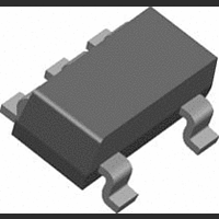
LMV7219M7 National Semiconductor, LMV7219M7 Datasheet - Page 9

LMV7219M7
Manufacturer Part Number
LMV7219M7
Description
Voltage Comparator IC
Manufacturer
National Semiconductor
Datasheet
1.LMV7219M7.pdf
(12 pages)
Specifications of LMV7219M7
No. Of Comparators
1
Response Time
7ns
No. Of Pins
5
Output Type
Push Pull
Single Supply Voltage Min (+v)
2.7V
Operating Voltage Max
5V
Operating Voltage Min
2.7V
Rail To Rail I/o Type
Rail Rail Outputs
Lead Free Status / RoHS Status
Contains lead / RoHS non-compliant
Available stocks
Company
Part Number
Manufacturer
Quantity
Price
Part Number:
LMV7219M7
Manufacturer:
NS/国半
Quantity:
20 000
Company:
Part Number:
LMV7219M7X
Manufacturer:
NS
Quantity:
2 695
Company:
Part Number:
LMV7219M7X
Manufacturer:
NATIONAL
Quantity:
1 112
Part Number:
LMV7219M7X
Manufacturer:
NS/国半
Quantity:
20 000
Additional Hysteresis
If additional hysteresis is desired, this can be done with the
addition of three resistors using positive feedback, as shown
in Figure 2. The positive feedback method slows the com-
parator response time. Calculate the resistor values as fol-
lows:
1) Select R3. The current through R3 should be greater than
the input bias current to minimize errors. The current through
R3 (I
possible output states when solving for R3, and use the
smaller of the two resulting resistor values. The two formulas
are:
2) Choose a hysteresis band required (V
3) Calculate R1, where R1 = R3 X(V
4) Choose the trip point for V
voltage (V
high as V
5) Calculate R2 as follows:
6) Verify the trip voltage and hysteresis as follows:
This method is recommended for additional hysteresis of up
to a few hundred millivolts. Beyond that, the impedance of
R3 is low enough to affect the bias string and adjustment of
R1 may be also required.
Circuit Layout and Bypassing
The LMV7219 requires high-speed layout. Follow these lay-
out guidelines:
1. Power supply bypassing is critical, and will improve sta-
bility and transient response. A decoupling capacitor such as
R3 = V
R3 = V
F
) at the trip point is (V
REF
CC
IN
THR
rises about the trip point.
FIGURE 2. Additional Hysteresis
- V
/I
) at which the comparator switches from low to
F
REF
/I
F
(when V
REF
(V
OUT
IN
- V
rising. This is the threshold
OUT
= V
OUT
) /R3. Consider the two
CC
HB
= 0)
/V
)
HB
CC
).
)
10105421
9
0.1µF ceramic should be placed as close as possible to V
pin. An additional 2.2µF tantalum capacitor may be required
for extra noise reduction.
2. Keep all leads short to reduce stray capacitance and lead
inductance. It will also minimize unwanted parasitic feedback
around the comparator.
3. The device should be soldered directly to the PC board
instead of using a socket.
4. Use a PC board with a good, unbroken low inductance
ground plane. Make sure ground paths are low-impedance,
especially were heavier currents are flowing.
5. Input traces should be kept away from output traces. This
can be achieved by running a topside ground plane between
the output and inputs.
6. Run the ground trace under the device up to the bypass
capacitor to shield the inputs from the outputs.
7. To prevent parasitic feedback when input signals are
slow-moving, a small capacitor of 1000pF or less can be
placed between the inputs. It can also help eliminate oscil-
lations in the transition region. However, this capacitor can
cause some degradation to tpd when the source impedance
is low.
Zero-Crossing Detector
The inverting input is connected to ground and the non-
inverting input is connected to 100mVp-p signal. As the
signal at the non-inverting input crosses 0V, the compara-
tor’s output Changes State.
Threshold Detector
Instead of tying the inverting input to 0V, the inverting input
can be tied to a reference voltage. The non-inverting input is
connected to the input. As the input passes the V
old, the comparator’s output changes state.
FIGURE 3. Zero-Crossing Detector
FIGURE 4. Threshold Detector
10105423
10105422
www.national.com
REF
thresh-
+


