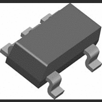
LMV7219M7 National Semiconductor, LMV7219M7 Datasheet - Page 5

LMV7219M7
Manufacturer Part Number
LMV7219M7
Description
Voltage Comparator IC
Manufacturer
National Semiconductor
Datasheet
1.LMV7219M7.pdf
(12 pages)
Specifications of LMV7219M7
No. Of Comparators
1
Response Time
7ns
No. Of Pins
5
Output Type
Push Pull
Single Supply Voltage Min (+v)
2.7V
Operating Voltage Max
5V
Operating Voltage Min
2.7V
Rail To Rail I/o Type
Rail Rail Outputs
Lead Free Status / RoHS Status
Contains lead / RoHS non-compliant
Available stocks
Company
Part Number
Manufacturer
Quantity
Price
Part Number:
LMV7219M7
Manufacturer:
NS/国半
Quantity:
20 000
Company:
Part Number:
LMV7219M7X
Manufacturer:
NS
Quantity:
2 695
Company:
Part Number:
LMV7219M7X
Manufacturer:
NATIONAL
Quantity:
1 112
Part Number:
LMV7219M7X
Manufacturer:
NS/国半
Quantity:
20 000
t
t
t
t
PD
SKEW
r
f
Symbol
5V Electrical Characteristics
Unless otherwise specified, all limits guaranteed for T
V
Note 1: Absolute Maximum Ratings indicate limits beyond which damage to the device may occur. Operating Ratings indicate conditions for which the device is
intended to be functional, but specific performance is not guaranteed. For guaranteed specifications and the test conditions, see the Electrical characteristics.
Note 2: Human body model, 1.5 kΩ in series with 100 pF. Machine model, 200Ω in series with 100 pF.
Note 3: Applies to both single-supply and split-supply operation. Continuous short circuit operation at elevated ambient temperature can result in exceeding the
maximum allowed junction temperature of 150˚C. Output currents in excess of
Note 4: The maximum power dissipation is a function of T
P
Note 5: Typical Values represent the most likely parametric norm.
Note 6: All limits are guaranteed by testing or statistical analysis.
Note 7: Propagation delay measurements made with 100 mV steps. Overdrive is measure relative to V
Note 8: Propagation Delay Skew is defined as absolute value of the difference between t
Note 9: Limiting input pin current is only necessary for input voltages that exceed absolute maximum input voltage ratings.
Note 10: The LMV7219 comparator has internal hysteresis. The trip points are the input voltage needed to change the output state in each direction. The offset
voltage is defined as the average of V
D
−
. Boldface limits apply at the temperature extremes.
= (T
J(MAX)
Propagation Delay
Propagation Delay Skew
Output Rise Time
Output Fall Time
- T
A
)/θ
JA
. All numbers apply for packages soldered directly into a PC board.
Parameter
trip +
and V
trip −
, while the hysteresis voltage is the difference of these two.
J(MAX)
(Continued)
Overdrive = 5 mV
V
Overdrive = 15mV
V
Overdrive = 50 mV
V
(Note 8)
10% to 90%
90% to 10%
CM
CM
CM
J
, θ
= 25˚C, V
JA
= 0V (Note 7)
= 0V (Note 7)
= 0V (Note 7)
, and T
Conditions
±
5
30mA over long term may adversely affect reliability.
A
. The maximum allowable power dissipation at any ambient temperature is
CM
= V
PDLH
+
/2, V
and t
+
PDHL
= 5V, V
Trip
.
.
(Note 5)
1.25
Typ
0.4
1.3
−
9
8
7
= 0V, C
L
= 10 pF and R
(Note 6)
Limit
20
19
L
>
www.national.com
1 MΩ to
Units
max
ns
ns
ns
ns


