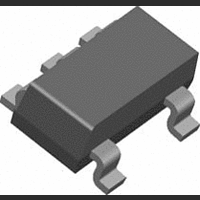
LMV331M7 National Semiconductor, LMV331M7 Datasheet - Page 7

LMV331M7
Manufacturer Part Number
LMV331M7
Description
Voltage Comparator IC
Manufacturer
National Semiconductor
Specifications of LMV331M7
No. Of Comparators
1
No. Of Pins
5
Peak Reflow Compatible (260 C)
No
Output Type
TTL/CMOS
No. Of Circuits
1
Leaded Process Compatible
No
Package / Case
5-SC70
Lead Free Status / RoHS Status
Contains lead / RoHS non-compliant
Available stocks
Company
Part Number
Manufacturer
Quantity
Price
Company:
Part Number:
LMV331M7
Manufacturer:
COOPER
Quantity:
600
Part Number:
LMV331M7
Manufacturer:
NS/国半
Quantity:
20 000
Company:
Part Number:
LMV331M7/NOPB
Manufacturer:
NS
Quantity:
276 000
Part Number:
LMV331M7/NOPB
Manufacturer:
TI/德州仪器
Quantity:
20 000
Company:
Part Number:
LMV331M7X
Manufacturer:
NS
Quantity:
5 321
Company:
Part Number:
LMV331M7X
Manufacturer:
NATIONAL
Quantity:
347
Part Number:
LMV331M7X
Manufacturer:
TI/德州仪器
Quantity:
20 000
Application Circuits
Basic Comparator
A basic comparator circuit is used for converting analog sig-
nals to a digital output. The LMV331/393/339 have an
open-collector output stage, which requires a pull-up resistor
to a positive supply voltage for the output to switch properly.
When the internal output transistor is off, the output voltage
will be pulled up to the external positive voltage.
The output pull-up resistor should be chosen high enough so
as to avoid excessive power dissipation yet low enough to
supply enough drive to switch whatever load circuitry is used
on the comparator output. On the LMV331/393/339 the
pull-up resistor should range between 1k to 10k .
The comparator compares the input voltage (V
non-inverting pin to the reference voltage (V
ing pin. If V
saturation voltage. On the other hand, if V
V
ref
, the output voltage (V
in
is less than V
ref
o
) is at V
, the output voltage (V
cc.
.
in
ref
is greater than
) at the invert-
o
in
) is at the
) at the
7
Comparator with Hysteresis
The basic comparator configuration may oscillate or produce
a noisy output if the applied differential input voltage is near
the comparator’s offset voltage. This usually happens when
the input signal is moving very slowly across the compara-
tor’s switching threshold. This problem can be prevented by
the addition of hysteresis or positive feedback.
Inverting Comparator with Hysteresis
The inverting comparator with hysteresis requires a three re-
sistor network that are referenced to the supply voltage V
of the comparator. When Vin at the inverting input is less
than V
parator (V
assume V
sistors can be represented as R
lower input trip voltage V
When V
low very close to ground. In this case the three network re-
sistors can be presented as R
per trip voltage V
The total hysteresis provided by the network is defined as
To assure that the comparator will always switch fully to V
and not be pulled down by the load the resistors values
should be chosen as follow:
a
, the voltage at the non-inverting node of the com-
in
in
o
is greater than Va (V
switches as high as V
<
FIGURE 1. Basic Comparator
V
a
a2
), the output voltage is high (for simplicity
is defined as
and R
R
pull-up
V
a
a1
= V
1
is defined as
>
<<
2
a1
//R
R
in
1
- V
pull-up
//R
3
R
cc
V
in series with R
load
a
). The three network re-
a2
3
), the output voltage is
in series with R
.
DS100080-4
DS100080-26
www.national.com
1
. The up-
2
. The
cc
cc


