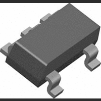
LMV331M7 National Semiconductor, LMV331M7 Datasheet - Page 10

LMV331M7
Manufacturer Part Number
LMV331M7
Description
Voltage Comparator IC
Manufacturer
National Semiconductor
Specifications of LMV331M7
No. Of Comparators
1
No. Of Pins
5
Peak Reflow Compatible (260 C)
No
Output Type
TTL/CMOS
No. Of Circuits
1
Leaded Process Compatible
No
Package / Case
5-SC70
Lead Free Status / RoHS Status
Contains lead / RoHS non-compliant
Available stocks
Company
Part Number
Manufacturer
Quantity
Price
Company:
Part Number:
LMV331M7
Manufacturer:
COOPER
Quantity:
600
Part Number:
LMV331M7
Manufacturer:
NS/国半
Quantity:
20 000
Company:
Part Number:
LMV331M7/NOPB
Manufacturer:
NS
Quantity:
276 000
Part Number:
LMV331M7/NOPB
Manufacturer:
TI/德州仪器
Quantity:
20 000
Company:
Part Number:
LMV331M7X
Manufacturer:
NS
Quantity:
5 321
Company:
Part Number:
LMV331M7X
Manufacturer:
NATIONAL
Quantity:
347
Part Number:
LMV331M7X
Manufacturer:
TI/德州仪器
Quantity:
20 000
www.national.com
Application Circuits
Pulse generator with variable duty cycle:
The pulse generator with variable duty cycle is just a minor
modification of the basic square wave generator. Providing a
separate charge and discharge path for capacitor C
ates a variable duty cycle. One path, through R
charge the capacitor and set the pulse width (t
path, R
between pulses (t
By varying resistor R
erator can be changed without changing the pulse width.
Similarly, by varying R
out affecting the time between pulses. Both controls will
change the frequency of the generator. The pulse width and
time between pulses can be found from:
Solving these equations for t
1
and D
1
FIGURE 7. Pulse Generator
will discharge the capacitor and set the time
2
).
1
, the time between pulses of the gen-
2
, the pulse width will be altered with-
t
t
1
2
= R
= R
1
4
5
C
C
and t
1
1
ln2
ln2
(Continued)
2
1
2
). The other
and D
1
gener-
DS100080-9
2
will
10
These terms will have a slight error due to the fact that V
is not exactly equal to 2/3 V
diode drop to:
Positive Peak Detector:
Positive peak detector is basically the comparator operated
as a unit gain follower with a large holding capacitor from the
output to ground. Additional transistor is added to the output
to provide a low impedance current source. When the output
of the comparator goes high, current is passed through the
transistor to charge up the capacitor. The only discharge
path will be the 1M ohm resistor shunting C1 and any load
that is connected to the output. The decay time can be al-
tered simply by changing the 1M ohm resistor. The output
should be used through a high impedance follower to a avoid
loading the output of the peak detector.
Negative Peak Detector:
For the negative detector, the output transistor of the com-
parator acts as a low impedance current sink. The only dis-
charge path will be the 1 M
ance used. Decay time is changed by varying the 1 M
resistor
FIGURE 9. Negative Peak Detector
FIGURE 8. Positive Peak Detector
CC
but is actually reduced by the
resistor and any load imped-
DS100080-18
DS100080-17
max


