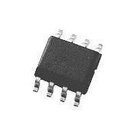
LMH6702MA National Semiconductor, LMH6702MA Datasheet - Page 3

LMH6702MA
Manufacturer Part Number
LMH6702MA
Description
Operational Amplifier (Op-Amp) IC
Manufacturer
National Semiconductor
Specifications of LMH6702MA
Op Amp Type
Low Distortion
No. Of Amplifiers
1
Bandwidth
720MHz
Slew Rate
3100V/µs
Supply Voltage Range
± 5V To ± 6V
Amplifier Case Style
SOIC
No. Of Pins
8
Number Of Channels
1
Common Mode Rejection Ratio (min)
45 dB
Input Offset Voltage
4.5 mV at +/- 5 V
Supply Current
16.1 mA at +/- 5 V
Maximum Operating Temperature
+ 85 C
Package / Case
SOIC-8 Narrow
Maximum Dual Supply Voltage
+/- 6 V
Minimum Operating Temperature
- 40 C
Lead Free Status / RoHS Status
Contains lead / RoHS non-compliant
Available stocks
Company
Part Number
Manufacturer
Quantity
Price
Part Number:
LMH6702MA
Manufacturer:
NS/国半
Quantity:
20 000
Part Number:
LMH6702MAX
Manufacturer:
NS/国半
Quantity:
20 000
INV
Static, DC Performance
V
DV
I
DI
I
DI
PSRR
CMRR
I
Miscellaneous Performance
R
C
R
V
CMIR
I
BN
BI
CC
O
Symbol
IO
OL
Electrical Characteristics
IN
IN
OUT
A
Note 1: Absolute Maximum Ratings indicate limits beyond which damage to the device may occur. Operating Ratings indicate conditions for which the device is
intended to be functional, but specific performance is not guaranteed. For guaranteed specifications, see the Electrical Characteristics tables.
Note 2: Electrical Table values apply only for factory testing conditions at the temperature indicated. Factory testing conditions result in very limited self-heating of
the device such that T
Min/Max ratings are based on production testing unless otherwise specified.
Note 3: The maximum output current (I
Note 4: Human body model: 1.5kΩ in series with 100pF. Machine model: 0Ω in series with 200pF.
Note 5: Slew Rate is the average of the rising and falling edges.
Note 6: Typical numbers are the most likely parametric norm. Bold numbers refer to over temperature limits.
Note 7: Negative input current implies current flowing out of the device.
Note 8: Drift determined by dividing the change in parameter at temperature extremes by the total temperature change.
Note 9: Harmonic distortion is strongly influenced by package type (SOT23-5 or SOIC). See Application Note section under "Harmonic Distortion" for more
information.
BN
BI
IO
V
= +2, V
Total Integrated Input Noise
Input Offset Voltage
Input Offset Voltage Average
Drift
Input Bias Current
Input Bias Current Average Drift
Input Bias Current
Input Bias Current Average Drift
Power Supply Rejection Ratio
Common Mode Rejection Ration
Supply Current
Input Resistance
Input Capacitance
Output Resistance
Output Voltage Range
Input Voltage Range
Output Current
S
=
±
5V, R
J
= T
Parameter
A
. No guarantee of parametric performance is indicated in the electrical tables under conditions of internal self-heating where T
L
= 100Ω, R
OUT
) is determined by device power dissipation limitations.
F
= 237Ω; unless specified
(Note 2) (Continued)
1MHz to 150MHz
(Note 8)
Non-Inverting (Note 7)
Non-Inverting (Note 8)
Inverting (Note 7)
Inverting (Note 8)
DC
DC
R
Non-Inverting
Non-Inverting
Closed Loop
R
Common Mode
L
L
= 100Ω
=
∞
Conditions
3
(Note 6)
±
±
±
11.0
10.0
Min
47
45
45
44
50
3.3
3.2
1.9
(Note 6)
±
±
±
12.5
Typ
−13
+40
−10
1.4
1.6
−6
−8
35
52
48
30
80
1.0
3.5
2.2
(Note 6)
±
±
Max
16.1
17.5
±
±
±
±
4.5
6.0
15
21
30
34
www.national.com
J
µV/˚C
nA/˚C
nA/˚C
Units
MΩ
mΩ
>
mV
mA
mA
µV
µA
µA
dB
dB
pF
V
V
T
A
.


