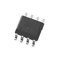
LM3477MM National Semiconductor, LM3477MM Datasheet - Page 16

LM3477MM
Manufacturer Part Number
LM3477MM
Description
Pulse Width Modulation (PWM) Controller IC
Manufacturer
National Semiconductor
Specifications of LM3477MM
Input Voltage Primary Min
2.95V
Mounting Type
Surface Mount
Topology
Buck (Step Down)
Control Mode
Current
Duty Cycle Max
93%
Input Voltage Primary Max
35V
Lead Free Status / RoHS Status
Contains lead / RoHS non-compliant
Available stocks
Company
Part Number
Manufacturer
Quantity
Price
Part Number:
LM3477MM
Manufacturer:
NS/国半
Quantity:
20 000
Part Number:
LM3477MM/NOPB
Manufacturer:
NS/国半
Quantity:
20 000
Part Number:
LM3477MMX
Manufacturer:
NS/国半
Quantity:
20 000
Company:
Part Number:
LM3477MMX/NOPB
Manufacturer:
TI
Quantity:
6 223
www.national.com
Design Section
tion). A convenient indicator of how much resonance exists is
quality factor Q. If Q is too high, subharmonic oscillations
could occur, if Q is too low, the current mode architecture
begins to act like a voltage mode architecture and the nec-
essary compensation becomes more complex. This is dis-
cussed in more detail in the COMPENSATION section, but
here it is important to calculate Q to be sure the selected
inductance will not cause problems to the stability of the
converter. The calculations below call for an inductance that
results in Q between 0.15 and 2. See the COMPENSATION
section if the chosen inductance enforces Q to be out of this
range. By default, no extra slope compensation is needed,
so R
Where,
V
I
V
Back solving for L gives a range for acceptable inductances
based on a range for Q:
It is recommended that:
Q(max) = 2, and
Q(min) = 0.15
Values for V
TERISTICS section.
Note: Adding slope compensation with R
current limit. An iterative process may be needed to meet
current limit and stability requirements, see PROGRAM-
MING CURRENT LIMIT/HYSTERETIC THRESHOLD sec-
tion.
Output Capacitor Selection
A capacitance between 47µF - 100µF is typically used. Skip
to ’Calculations for the Output Capacitance’ for minimum
capacitance calculations.
OUT
Q
SEN
*
SL
= V
R
= Voltage across the sense resistor ) I
DS(ON).
= 0. In general, a Q between 0.5 and 1 is optimal.
DS
SL
of the MOSFET when it is conducting
can be found in the ELECTRICAL CHARAC-
D’ = 1−D
(Continued)
SL
will decrease the
OUT
x R
SN
16
Type of output capacitors
Different type of capacitors often have different combinations
of capacitance, equivalent series resistance (ESR), and volt-
age ratings. High-capacitance multi-layer ceramic capacitors
(MLCCs) have a very low ESR, typically 12mΩ, but also
relatively low capacitance and low voltage ratings. Tantalum
capacitors can have fairly low ESR, such as 18mΩ, and high
capacitance (up to 1mF) at higher voltage ratings than ML-
CCs. Aluminum capacitors offer high capacitance and rela-
tively low ESR and are available in high voltage ratings.
OSCON capacitors can achieve ESR values that are even
lower than those of MLCCs and with higher capacitance, but
the voltage ratings are low. Other tradeoffs in capacitor
technology include temperature stability, surge current capa-
bility, and capacitance density (physical size vs. capaci-
tance).
Output Capacitor Considerations
Skip to the ’Calculations for the output capacitor’ subsection
if a quick design is desired. While it is generally desired to
use as little output capacitance as possible to keep costs
down, the output capacitor should be chosen with care as it
directly affects the ripple component of the output voltage as
well as other components in the design. The output voltage
ripple is directly proportional to the ESR of the output capaci-
tor (see POWER INDUCTOR section). Therefore, designs
requiring low output voltage ripple should have an output
capacitor with low ESR. Choosing a capacitor with low ESR
has the additional benefit of requiring one less component in
the compensation network, as discussed in the Compensa-
tion section.
In addition to the output voltage ripple, the output capacitor
directly affects the output voltage overshoot in a load tran-
sient. Two transients are possible: an unloading transient
and a loading transient. An unloading transient occurs when
the load current transitions to a higher current, and charge is
unloaded from the output capacitor. A loading transient is
when the load transitions to a lower current, and charge is
loaded to the output capacitor. How the output voltage reacts
during these transitions is known as the transient response.
Both the capacitance and the ESR of the output capacitor
will affect the transient response.
The control loop of the LM3477/A can be made fast enough
to saturate the duty cycle when the worst case lode transient
occurs. This means the duty cycle jumps to D
depending on the type of load transient. In a loading tran-
sient, as shown in Figure 9, the duty cycle drops to D
while the inductor current falls to match the load current.
During this time, the regulator is heavily dependent on the
output capacitors to handle the load transient. The initial
overshoot is caused by the ESR of the output capacitors.
FIGURE 9. A Loading Transient
MIN
200033B9
or D
MAX
MIN
,


