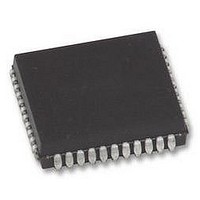
P89V51RB2FA NXP Semiconductors, P89V51RB2FA Datasheet - Page 38

P89V51RB2FA
Manufacturer Part Number
P89V51RB2FA
Description
MCU 8BIT 80C51 16K FLASH, PLCC44
Manufacturer
NXP Semiconductors
Datasheet
1.P89V51RC2FBC557.pdf
(80 pages)
Specifications of P89V51RB2FA
Controller Family/series
(8051) 8052
Core Size
8bit
No. Of I/o's
32
Program Memory Size
16KB
Ram Memory Size
1KB
Cpu Speed
40MHz
Oscillator Type
External Only
No. Of Timers
4
No. Of Pwm
RoHS Compliant
Available stocks
Company
Part Number
Manufacturer
Quantity
Price
Company:
Part Number:
P89V51RB2FA
Manufacturer:
NXP
Quantity:
1 000
Company:
Part Number:
P89V51RB2FA
Manufacturer:
NXP
Quantity:
2 000
Part Number:
P89V51RB2FA
Manufacturer:
NXP/恩智浦
Quantity:
20 000
Part Number:
P89V51RB2FA (FLA
Manufacturer:
NXP/恩智浦
Quantity:
20 000
Company:
Part Number:
P89V51RB2FA,529
Manufacturer:
NXP Semiconductors
Quantity:
10 000
Company:
Part Number:
P89V51RB2FAЈ¬529
Manufacturer:
NXP
Quantity:
150
NXP Semiconductors
P89V51RB2_RC2_RD2_5
Product data sheet
6.6.2 Mode 1
6.6.3 Mode 2
6.6.4 Mode 3
10 bits are transmitted (through TXD) or received (through RXD): a start bit (logical 0), 8
data bits (LSB first), and a stop bit (logical 1). When data is received, the stop bit is stored
in RB8 in Special Function Register SCON. The baud rate is variable and is determined
by the Timer
11 bits are transmitted (through TXD) or received (through RXD): start bit (logical 0), 8
data bits (LSB first), a programmable 9th data bit, and a stop bit (logical 1). When data is
transmitted, the 9th data bit (TB8 in SCON) can be assigned the value of 0 or (e.g. the
parity bit (P, in the PSW) could be moved into TB8). When data is received, the 9th data
bit goes into RB8 in Special Function Register SCON, while the stop bit is ignored. The
baud rate is programmable to either
by the SMOD1 bit in PCON.
11 bits are transmitted (through TXD) or received (through RXD): a start bit (logical 0), 8
data bits (LSB first), a programmable 9th data bit, and a stop bit (logical 1). In fact, mode 3
is the same as mode 2 in all respects except baud rate. The baud rate in mode 3 is
variable and is determined by the Timer
Table 25.
Bit addressable; Reset value: 00H
Table 26.
Bit
7
6
5
4
3
Bit
Symbol
SCON - Serial port control register (address 98H) bit allocation
SCON - Serial port control register (address 98H) bit description
SM0/FE
Symbol
SM0/FE
SM1
SM2
REN
TB8
1
2
7
overflow rate.
Rev. 05 — 12 November 2009
SM1
6
Description
The usage of this bit is determined by SMOD0 in the PCON register. If
SMOD0 = 0, this bit is SM0, which with SM1, defines the serial port
mode. If SMOD0 = 1, this bit is FE (Framing Error). FE is set by the
receiver when an invalid stop bit is detected. Once set, this bit cannot
be cleared by valid frames but can only be cleared by software. (Note:
It is recommended to set up UART mode bits SM0 and SM1 before
setting SMOD0 to ‘1’.)
With SM0, defines the serial port mode (see
Enables the multiprocessor communication feature in modes 2 and 3.
In mode 2 or 3, if SM2 is set to ‘1’, then RI will not be activated if the
received 9th data bit (RB8) is ‘0’. In mode 1, if SM2 = 1 then RI will not
be activated if a valid stop bit was not received. In mode 0, SM2
should be ‘0’.
Enables serial reception. Set by software to enable reception. Clear by
software to disable reception.
The 9th data bit that will be transmitted in modes 2 and 3. Set or clear
by software as desired.
SM2
5
1
16
or
1
2
1
REN
overflow rate.
P89V51RB2/RC2/RD2
32
4
of the CPU clock frequency, as determined
8-bit microcontrollers with 80C51 core
TB8
3
RB8
2
Table 27
© NXP B.V. 2009. All rights reserved.
TI
below).
1
38 of 80
RI
0


