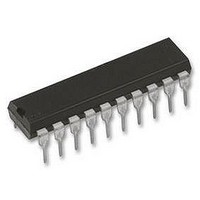
P89LPC922FN NXP Semiconductors, P89LPC922FN Datasheet - Page 39

P89LPC922FN
Manufacturer Part Number
P89LPC922FN
Description
IC, MCU 8BIT 80C51 8K FLASH, DIP20
Manufacturer
NXP Semiconductors
Datasheet
1.P89LPC922FN.pdf
(46 pages)
Specifications of P89LPC922FN
Controller Family/series
(8051) 8052
Core Size
8bit
No. Of I/o's
18
Program Memory Size
8KB
Ram Memory Size
256Byte
Cpu Speed
18MHz
Oscillator Type
External, Internal
No. Of Timers
4
No. Of
RoHS Compliant
Available stocks
Company
Part Number
Manufacturer
Quantity
Price
Company:
Part Number:
P89LPC922FN
Manufacturer:
NICHICON
Quantity:
32 000
Part Number:
P89LPC922FN
Manufacturer:
NXP/恩智浦
Quantity:
20 000
Philips Semiconductors
Table 10:
V
T
[1]
[2]
9397 750 14469
Product data
Symbol
f
f
f
t
f
Glitch filter
External clock
t
t
t
t
Shift register (UART mode 0)
t
t
t
t
t
RCOSC
WDOSC
osc
CLCL
CLKP
CHCX
CLCX
CLCH
CHCL
XLXL
QVXH
XHQX
XHDX
DVXH
amb
DD
= 3.0 V to 3.6 V unless otherwise specified.
Parameters are valid over operating temperature range unless otherwise specified. Parts are tested to 2 MHz, but are guaranteed to
operate down to 0 Hz.
When using an oscillator frequency above 12 MHz, the reset input function of P1.5 must be enabled. An external circuit is required to
hold the device in reset at power-up until V
minimum specified operating voltage. When using an oscillator frequency above 12 MHz, in some applications, an external brownout
detect circuit may be required to hold the device in reset when V
= 40 C to +85 C for industrial, unless otherwise specified.
AC characteristics
Parameter
internal RC oscillator frequency
(nominal f = 7.3728 MHz)
internal Watchdog oscillator
frequency (nominal f = 400 kHz)
oscillator frequency
clock cycle
CLKLP active frequency
glitch rejection, P1.5/RST pin
signal acceptance, P1.5/RST pin
glitch rejection, any pin except
P1.5/RST
signal acceptance, any pin except
P1.5/RST
HIGH time
LOW time
rise time
fall time
serial port clock cycle time
output data set-up to clock rising
edge
output data hold after clock rising
edge
input data hold after clock rising edge
input data valid to clock rising edge
DD
has reached its specified level. When system power is removed V
Rev. 08 — 15 December 2004
Conditions
trimmed to 1%
at T
see
see
see
see
see
amb
Figure 13
Figure 13
Figure 13
Figure 13
Figure 13
= 25 C
DD
falls below the minimum specified operating voltage.
P89LPC920/921/922/9221
[1]
8-bit microcontrollers with two-clock 80C51 core
[2]
Variable clock
Min
7.189
320
0
55
0
-
125
-
50
22
22
-
-
16 t
13 t
-
-
150
CLCL
CLCL
Max
7.557
520
18
-
8
50
-
15
-
t
t
5
5
-
-
t
0
-
CLCL
CLCL
CLCL
+ 20
© Koninklijke Philips Electronics N.V. 2004. All rights reserved.
t
t
CLCX
CHCX
f
Min
7.189
320
-
-
-
-
125
-
50
22
22
-
-
888
722
-
-
150
osc
DD
= 18 MHz
will fall below the
Max
7.557
520
-
-
-
50
-
15
-
-
-
5
5
-
-
75
0
-
39 of 46
Unit
MHz
kHz
MHz
ns
MHz
ns
ns
ns
ns
ns
ns
ns
ns
ns
ns
ns
ns
ns


