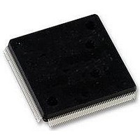
LFXP2-17E-5QN208C8W LATTICE SEMICONDUCTOR, LFXP2-17E-5QN208C8W Datasheet - Page 14

LFXP2-17E-5QN208C8W
Manufacturer Part Number
LFXP2-17E-5QN208C8W
Description
FPGA, 17K LUTS, 146 IO, DSP, 208PQFP
Manufacturer
LATTICE SEMICONDUCTOR
Series
LatticeXP2r
Datasheet
1.LFXP2-5E-5TN144C.pdf
(93 pages)
Specifications of LFXP2-17E-5QN208C8W
No. Of Macrocells
8500
Family Type
LatticeXP2
No. Of Speed Grades
5
No. Of I/o's
146
Clock Management
PLL
Core Supply Voltage Range
1.14V To 1.26V
I/o Supply
RoHS Compliant
- Current page: 14 of 93
- Download datasheet (2Mb)
Lattice Semiconductor
Edge Clock Sources
Edge clock resources can be driven from a variety of sources at the same edge. Edge clock resources can be
driven from adjacent edge clock PIOs, primary clock PIOs, PLLs and clock dividers as shown in Figure 2-8.
Figure 2-8. Edge Clock Sources
Note: This diagram shows sources for the XP2-17 device. Smaller LatticeXP2 devices have two GPLLs.
From Routing
From Routing
Sources for left edge clocks
Input
Input
PLL
PLL
Clock
Clock
Input
Input
GPLL
GPLL
CLKOP
CLKOS
CLKOP
CLKOS
Routing
Routing
From
From
Eight Edge Clocks (ECLK)
Two Clocks per Edge
Clock Input
Clock Input
2-11
Clock Input
Clock Input
Routing
Routing
From
From
Sources for top
bottom edge
Sources for
edge clocks
clocks
LatticeXP2 Family Data Sheet
Sources for right edge clocks
CLKOP
CLKOS GPLL
CLKOP
CLKOS GPLL
Architecture
From Routing
From Routing
Clock
Clock
Input
Input
Input
Input
PLL
PLL
Related parts for LFXP2-17E-5QN208C8W
Image
Part Number
Description
Manufacturer
Datasheet
Request
R

Part Number:
Description:
IC, LATTICEXP2 FPGA, 435MHZ, FPBGA-484
Manufacturer:
LATTICE SEMICONDUCTOR
Datasheet:

Part Number:
Description:
Development Tools & Eval/Demo Boards
Manufacturer:
LATTICE SEMICONDUCTOR
Datasheet:
Part Number:
Description:
FPGA LatticeXP2 Family 17000 Cells Flash Technology 1.2V 484-Pin FBGA
Manufacturer:
LATTICE SEMICONDUCTOR
Datasheet:
Part Number:
Description:
FPGA LatticeXP2 Family 17000 Cells Flash Technology 1.2V 484-Pin FBGA
Manufacturer:
LATTICE SEMICONDUCTOR
Datasheet:
Part Number:
Description:
FPGA LatticeXP2 Family 17000 Cells Flash Technology 1.2V 484-Pin FBGA
Manufacturer:
LATTICE SEMICONDUCTOR
Datasheet:
Part Number:
Description:
Latticexp2 Fpga Data Sheets
Manufacturer:
Lattice Semiconductor Corp.
Datasheet:

Part Number:
Description:
FPGA - Field Programmable Gate Array 5K LUTs 146I/O Inst- on DSP 1.2V -5 Spd
Manufacturer:
Lattice
Datasheet:

Part Number:
Description:
FPGA - Field Programmable Gate Array 5K LUTs 172I/O Inst- on DSP 1.2V -5 Spd
Manufacturer:
Lattice
Datasheet:

Part Number:
Description:
FPGA - Field Programmable Gate Array 5K LUTs 100I/O Inst- on DSP 1.2V -5 Spd
Manufacturer:
Lattice
Datasheet:
Part Number:
Description:
ISPLSI2032-80LT44Lattice Semiconductor [In-System Programmable High Density PLD]
Manufacturer:
Lattice Semiconductor Corp.
Datasheet:
Part Number:
Description:
IC PROGRAMMED LATTICE GAL 16V8
Manufacturer:
Lattice Semiconductor Corp.
Datasheet:
Part Number:
Description:
357-036-542-201 CARDEDGE 36POS DL .156 BLK LOPRO
Manufacturer:
Lattice Semiconductor Corp.
Datasheet:
Part Number:
Description:
357-036-542-201 CARDEDGE 36POS DL .156 BLK LOPRO
Manufacturer:
Lattice Semiconductor Corp.
Datasheet:
Part Number:
Description:
357-036-542-201 CARDEDGE 36POS DL .156 BLK LOPRO
Manufacturer:
Lattice Semiconductor Corp.
Datasheet:
Part Number:
Description:
357-036-542-201 CARDEDGE 36POS DL .156 BLK LOPRO
Manufacturer:
Lattice Semiconductor Corp.
Datasheet:


