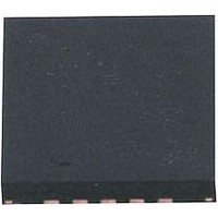
LTC5540IUH#PBF Linear Technology, LTC5540IUH#PBF Datasheet - Page 14

LTC5540IUH#PBF
Manufacturer Part Number
LTC5540IUH#PBF
Description
IC, DOWN CONVERTING MIXER 1.3GHZ, QFN-20
Manufacturer
Linear Technology
Datasheet
1.LTC5540IUHPBF.pdf
(16 pages)
Specifications of LTC5540IUH#PBF
Frequency Range
600MHz To 1.3GHz
Supply Voltage Range
3.1V To 3.5V
Rf Ic Case Style
QFN
No. Of Pins
20
Operating Temperature Range
-40°C To +85°C
Rf Type
GSM, LTE, WCDMA, WiMax
Operating Supply Voltage
3.3V
Operating Temperature (min)
-40C
Operating Temperature (max)
85C
Operating Temperature Classification
Industrial
Lead Free Status / RoHS Status
Lead free / RoHS Compliant
Lead Free Status / RoHS Status
Lead free / RoHS Compliant
Available stocks
Company
Part Number
Manufacturer
Quantity
Price
LTC5540
applicaTions inForMaTion
The IFBIAS pin (pin 20) is available for reducing the DC
current consumption of the IF amplifier, at the expense of
IIP3. This pin should be left open-circuited for optimum
performance. The internal bias circuit produces a 4mA
reference for the IF amplifier, which causes the amplifier
to draw approximately 96mA. If resistor R1 is connected
to pin 20 as shown in Figure 7, a portion of the reference
current can be shunted to ground, resulting in reduced
IF amplifier current. For example, R1 = 1kΩ will shunt
away 1.5mA from pin 20 and the IF amplifier current will
be reduced by 38% to approximately 59mA. The nominal,
open-circuit DC voltage at pin 20 is 2.1V. Table 6 lists RF
performance at 900MHz versus IF amplifier current.
Table 6. Mixer Performance with Reduced IF Amplifier Current
(RF = 900MHz, High-Side LO, IF = 190MHz, V
(RF = 900MHz, Low-Side LO, IF = 190MHz, V
Shutdown Interface
Figure 11 shows a simplified schematic of the SHDN pin
interface. To disable the chip, the SHDN voltage must be
higher than 3.0V. If the shutdown function is not required,
the SHDN pin should be connected directly to GND. The
voltage at the SHDN pin should never exceed the power
supply voltage (V
occur, the supply current could be sourced through the
ESD diode, potentially damaging the IC.
OPEN
OPEN
(kΩ)
(kΩ)
4.7
2.2
4.7
2.2
R1
R1
1
1
(mA)
(mA)
I
I
CCIF
CCIF
96
86
77
59
96
86
77
59
CC
) by more than 0.3V. If this should
(dB)
(dB)
7.9
7.7
7.6
7.3
7.0
6.9
6.8
6.3
G
G
C
C
(dBm)
(dBm)
25.9
25.3
24.7
23.0
24.4
23.4
23.2
22.4
IIP3
IIP3
CC
CC
(dBm)
(dBm)
P1dB
P1dB
11.0
11.1
11.3
10.8
11.0
11.0
11.1
10.5
= V
= V
CCIF
CCIF
= 3.3V)
= 3.3V)
(dB)
(dB)
10.6
10.6
10.6
10.5
9.9
9.9
9.9
9.8
NF
NF
The SHDN pin must be pulled high or low. If left floating,
then the on/off state of the IC will be indeterminate. If a
three-state condition can exist at the SHDN pin, then a
pull-up or pull-down resistor must be used.
Supply Voltage Ramping
Fast ramping of the supply voltage can cause a current
glitch in the internet ESD protection circuits. Depending on
the supply inductance, this could result in a supply voltage
transient that exceeds the maximum rating. A supply voltage
ramp time of greater than 1ms is recommended.
6
5
V
SHDN
CC2
Figure 11. Shutdown Input Circuit
500
LTC5540
5540 F11
5540f


