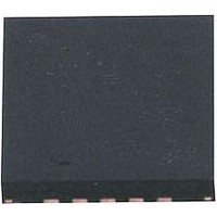
LTC5540IUH#PBF Linear Technology, LTC5540IUH#PBF Datasheet - Page 10

LTC5540IUH#PBF
Manufacturer Part Number
LTC5540IUH#PBF
Description
IC, DOWN CONVERTING MIXER 1.3GHZ, QFN-20
Manufacturer
Linear Technology
Datasheet
1.LTC5540IUHPBF.pdf
(16 pages)
Specifications of LTC5540IUH#PBF
Frequency Range
600MHz To 1.3GHz
Supply Voltage Range
3.1V To 3.5V
Rf Ic Case Style
QFN
No. Of Pins
20
Operating Temperature Range
-40°C To +85°C
Rf Type
GSM, LTE, WCDMA, WiMax
Operating Supply Voltage
3.3V
Operating Temperature (min)
-40C
Operating Temperature (max)
85C
Operating Temperature Classification
Industrial
Lead Free Status / RoHS Status
Lead free / RoHS Compliant
Lead Free Status / RoHS Status
Lead free / RoHS Compliant
Available stocks
Company
Part Number
Manufacturer
Quantity
Price
applicaTions inForMaTion
LTC5540
Introduction
The LTC5540 consists of a high linearity passive double-
balanced mixer core, IF buffer amplifier, high speed single-
pole double-throw (SPDT) LO switch, LO buffer amplifier
and bias/enable circuits. See Pin Functions section for a
description of each pin function. The RF and LO inputs
are single-ended. The IF output is differential. Low-side or
high-side LO injection can be used. The evaluation circuit,
shown in Figure 1, utilizes bandpass IF output matching and
an IF transformer to realize a 50Ω single-ended IF output.
The evaluation board layout is shown in Figure 2.
RF Input
The mixer’s RF input, shown in Figure 3, is connected to
the primary winding of an integrated transformer. A 50Ω
match is realized when a series capacitor, C1, is connected
to the RF input. C1 is also needed for DC blocking if the
RF source has DC voltage present, since the primary side
of the RF transformer is DC-grounded internally. The DC
resistance of the primary is approximately 5Ω.
The secondary winding of the RF transformer is internally
connected to the passive mixer. The center-tap of the
transformer secondary is connected to pin 3 (CT) to allow
the connection of bypass capacitor, C2. The value of C2
is LO frequency-dependent. C2 should be located within
0
Figure 2. Evaluation Board Layout
5540 F02
2mm of pin 3 for proper high-frequency decoupling. The
nominal DC voltage on the CT pin is 1.2V.
For the RF input to be properly matched, the selected
LO input must be driven. The values of C1 and C2 can
be chosen to optimize the performance for high-side
or low-side LO (see the table in Figure 1). For high-side
applications, a broadband input match is realized with
C1 = 5.6pF. The measured input return loss is shown in
Figure 4 for LO frequencies of 700MHz, 1090MHz and
1200MHz. As shown in Figure 4, the RF input impedance
is dependent on LO frequency, although a single value of
C1 is adequate to cover a wide RF range.
RF
IN
–10
–15
–20
–25
C1
–5
0
600
Figure 4. RF Input Return Loss
C2
Figure 3. RF Input Schematic
2
3
700
RF
CT
800
FREQUENCY (MHz)
900
1000
LO = 700MHz
LO = 1090MHz
LO = 1200MHz
TO MIXER
C1 = 5.6pF
LTC5540
1100
5541 F04
1200
5540 F03
5540f


