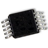
LM3481MM National Semiconductor, LM3481MM Datasheet - Page 5

LM3481MM
Manufacturer Part Number
LM3481MM
Description
IC, BOOST, CNTRL, 10MSOP
Manufacturer
National Semiconductor
Datasheet
1.LM3481EVALNOPB.pdf
(22 pages)
Specifications of LM3481MM
Primary Input Voltage
48V
No. Of Outputs
1
Output Current
1A
Voltage Regulator Case Style
MSOP
No. Of Pins
10
Operating Temperature Range
-40°C To +125°C
Svhc
No SVHC (15-Dec-2010)
Lead Free Status / RoHS Status
Lead free / RoHS Compliant
Available stocks
Company
Part Number
Manufacturer
Quantity
Price
Part Number:
LM3481MM
Manufacturer:
TI/德州仪器
Quantity:
20 000
Company:
Part Number:
LM3481MM/NOPB
Manufacturer:
TI
Quantity:
12 000
Part Number:
LM3481MMX
Manufacturer:
NS/国半
Quantity:
20 000
Company:
Part Number:
LM3481MMX/NOPB
Manufacturer:
TI
Quantity:
12 000
Note 1: Absolute Maximum Ratings are limits beyond which damage to the device may occur. Operating Ratings indicates conditions for which the device is
intended to be functional, but does not guarantee specific performance limits. For guaranteed specifications and test conditions, see the Electrical Characteristics.
The guaranteed specifications apply only for the test conditions.
Note 2: The human body model is a 100 pF capacitor discharged through a 1.5kΩ resistor into each pin.
Note 3: All limits are guaranteed at room temperature (standard type face) and at temperature extremes (bold type face). All room temperature limits are 100%
tested. All limits at temperature extremes are guaranteed via correlation using standard Statistical Quality Control (SQC) methods. All limits are used to calculate
Average Outgoing Quality Level (AOQL).
Note 4: Typical numbers are at 25°C and represent the most likely norm.
Note 5: The FA/SYNC/SD pin should be pulled to V
limit for the Output = High longer than 30 µs to keep the regulator off and must be below the minimum limit for Output = Low to keep the regulator on.
Note 6: The drive pin voltage, V
equal to 6V.
Note 7: The over-voltage protection is specified with respect to the feedback voltage. This is because the over-voltage protection tracks the feedback voltage.
The over-voltage threshold can be calculated by adding the feedback voltage (V
Note 8: For this test, the FA/SYNC/SD Pin is pulled to ground using a 40 kΩ resistor .
Note 9: For this test, the FA/SYNC/SD Pin is pulled to 3V using a 40 kΩ resistor.
Typical Performance Characteristics
Efficiency vs. Load Current (3.3V
Comp Pin Voltage vs. Load Current
DR
, is equal to the input voltage when input voltage is less than 6V. V
IN
IN
through a resistor to turn the regulator off. The voltage on the FA/SYNC/SD pin must be above the max
and 12V
20136548
20136546
OUT
)
5
Unless otherwise specified, V
FB
) to the over-voltage protection specification.
Efficiency vs. Load Current (5V
Switching Frequency vs. R
DR
is equal to 6V when the input voltage is greater than or
IN
= 12V, T
J
IN
= 25°C.
and 12V
FA
20136549
20136547
OUT
www.national.com
)


