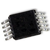
LM3481MM National Semiconductor, LM3481MM Datasheet - Page 11

LM3481MM
Manufacturer Part Number
LM3481MM
Description
IC, BOOST, CNTRL, 10MSOP
Manufacturer
National Semiconductor
Datasheet
1.LM3481EVALNOPB.pdf
(22 pages)
Specifications of LM3481MM
Primary Input Voltage
48V
No. Of Outputs
1
Output Current
1A
Voltage Regulator Case Style
MSOP
No. Of Pins
10
Operating Temperature Range
-40°C To +125°C
Svhc
No SVHC (15-Dec-2010)
Lead Free Status / RoHS Status
Lead free / RoHS Compliant
Available stocks
Company
Part Number
Manufacturer
Quantity
Price
Part Number:
LM3481MM
Manufacturer:
TI/德州仪器
Quantity:
20 000
Company:
Part Number:
LM3481MM/NOPB
Manufacturer:
TI
Quantity:
12 000
Part Number:
LM3481MMX
Manufacturer:
NS/国半
Quantity:
20 000
Company:
Part Number:
LM3481MMX/NOPB
Manufacturer:
TI
Quantity:
12 000
A more general equation for the slope compensation ramp,
M
R
It is good design practice to only add as much slope com-
pensation as needed to avoid subharmonic oscillation. Addi-
tional slope compensation minimizes the influence of the
sensed current in the control loop. With very large slope com-
pensation the control loop characteristics are similar to a
voltage mode regulator which compares the error voltage to
a saw tooth waveform rather than the inductor current.
SL
FIGURE 5. Increasing the Slope of the Compensation
C
, is shown below to include ΔV
.
FIGURE 6. ΔV
M
C
= (V
SL
Ramp
+ ΔV
SL
SL
SL
vs R
) x f
caused by the resistor
S
SL
20136551
20136513
11
FREQUENCY ADJUST/SYNCHRONIZATION/SHUTDOWN
The switching frequency of the LM3481 can be adjusted be-
tween 100 kHz and 1 MHz using a single external resistor.
This resistor must be connected between the FA/SYNC/SD
pin and ground, as shown in
ical performance characteristics to determine the value of the
resistor required for a desired switching frequency.
The following equation can also be used to estimate the fre-
quency adjust resistor.
Where f
The LM3481 can be synchronized to an external clock. The
external clock must be connected between the FA/SYNC/SD
pin and ground, as shown in
resistor may remain connected while synchronizing a signal,
therefore if there is a loss of signal, the switching frequency
will be set by the frequency adjust resistor.
It is also necessary to have the width of the synchronization
pulse narrower than the duty cycle of the converter and to
have the synchronization pulse width
The FA/SYNC/SD pin also functions as a shutdown pin. If a
high signal (refer to the electrical characteristics section for
definition of high signal) appears on the FA/SYNC/SD pin, the
LM3481 stops switching and goes into a low current mode.
The total supply current of the IC reduces to 5 µA, typically,
under these conditions.
Figure 9
down function when operating in frequency adjust mode and
synchronization mode respectively. In frequency adjust
mode, connecting the FA/SYNC/SD pin to ground forces the
clock to run at a certain frequency. Pulling this pin high shuts
down the IC. In frequency adjust or synchronization mode, a
high signal for more than 30 µs shuts down the IC.
S
and
is in kHz and R
Figure 10
shows an implementation of a shut-
FA
in kΩ.
Figure
Figure
7. Please refer to the typ-
8. The frequency adjust
≥
300 ns.
www.national.com


