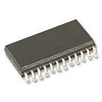
LM2650M-ADJ National Semiconductor, LM2650M-ADJ Datasheet - Page 3

LM2650M-ADJ
Manufacturer Part Number
LM2650M-ADJ
Description
DC/DC CONVERTER, ADJ, 2650, SOIC24
Manufacturer
National Semiconductor
Datasheet
1.LM2650M-ADJ.pdf
(11 pages)
Specifications of LM2650M-ADJ
Primary Input Voltage
18V
No. Of Outputs
1
Output Voltage
16V
Output Current
3A
Voltage Regulator Case Style
SOIC
No. Of Pins
24
Operating Temperature Range
-40°C To +125°C
Svhc
No SVHC
Lead Free Status / RoHS Status
Lead free / RoHS Compliant
Available stocks
Company
Part Number
Manufacturer
Quantity
Price
Company:
Part Number:
LM2650M-ADJ
Manufacturer:
NS
Quantity:
1 438
Company:
Part Number:
LM2650M-ADJ
Manufacturer:
NATIONAL
Quantity:
425
Part Number:
LM2650M-ADJ
Manufacturer:
NS/国半
Quantity:
20 000
Company:
Part Number:
LM2650M-ADJ/NOPB
Manufacturer:
TI
Quantity:
15 540
V
V
I
I
I
R
R
I
I
I
F
F
D
Q
QS
QSD
L HS
L LS
LIMIT
V
type apply for T
Operating Ratings.
1
2
OSC
MAX
OUT
REF
DS(on)
DS(on)
MAX
Electrical Characteristics
Absolute Maximum Ratings
If Military/Aerospace specified devices are required,
please contact the National Semiconductor Sales Office/
Distributors for availability and specifications.
(All voltages are referenced to the PGND and GND pins.)
DC Voltage at PV
DC Voltage at SD, SLEEP LOGIC
and SYNC
DC current into SW
Junction Temperature
DC Power Dissipation (Note 2)
Storage Temperature
PVIN
Symbol
= 15V, V
HS
LS
Output Voltage
System Efficiency
System Efficiency
Reference Voltage
Quiescent Current in PWM
mode
Quiescent Current in Sleep
mode
Quiescent Current in Shutdown
mode
DC On-Resistance
Drain-to-Source of the
High-Side Power Switch
DC On-Resistance
Drain-to-Source of the
Low-Side Power Switch
Leakage current of the
High-Side Power Switch
Leakage current of the
Low-Side Power Switch
Active Current Limit of the
High-Side Power Switch
Oscillator Frequency
Maximum Oscillator Frequency
Maximum Duty Cycle
SLEEP LOGIC
A
= T
IN
J
and V
= +25˚C. Limits appearing in boldface type apply over the full junction temperature range shown under
Parameter
IN
= 0V and V
SD
= 0V unless superseded under Conditions. Typicals and limits appearing in plain
Limited by the IC
−65˚C to +150˚C
(Note 1)
R1 = 75 k , 1%,
R2 = 25 k , 1%,
7.5V
0.12A
I
F
I
F
V
V
−20mV (Note 8)
IV
V
V
(Note 8)
I
V
V
V
I
V
V
V
V
V
V
V
V
V
V
I
V
V
F
LOAD
LOAD
DS
DS
FREQ ADJ
OSC
OSC
OSC
SLEEPLOGIC
FB
SLEEPLOGIC
SD
SLEEPLOGIC
FB
BOOT
FB
PVIN
SD
PVIN
SD
PVIN
BOOT
FB
SLEEPLOGIC
FB
FB
FB
FB
= 1A,
= 1A,
= V
= 3V,
= 3V
= 3V,
= V
= V
= V
1.28W
= 3V
= 3V
= 3V
±
= V
Not Adjusted
Not Adjusted
Not Adjusted
= 1A, T
= 3A, T
= 18V, V
= 18V, V
= 15V,
7.5A
20V
15V
V
= 24V
= 24V,
REF
REF
REF
REF
I
PVIN
REF
LOAD
Conditions
= 100µA,(Note 9)
−20 mV
−20 mV
−20 mV,
−20mV,
= 3V (Note 7)
= 3V (Note 8)
= 3V,
= 3V,
A
A
3
SW
SW
18V
= 25˚C,
= 25˚C,
3A
Soldering Time, Temperature (Note
3)
ESD Susceptibility (Note 4)
Operating Ratings
Supply Voltage Range (PV
V
Junction Temperature Range
= 0V,
= 18V,
IN
Wave (4 seconds)
Infrared (10 seconds)
Vapor Phase (75 seconds)
)
Typ (Note 5)
5.00
1.25
850
130
125
100
315
4.0
5.5
94
89
95
90
97
9
IN
and
(Note 1)
Limit (Note 6)
1.281/1.294
1.219/1.206
4.80/4.75
5.20/5.25
1.35/1.60
6.50/7.0
170/245
175/245
100/105
270/260
360/370
20/25
80/75
94/93
210
3.5
7.5
10
−40˚C to +125˚C
www.national.com
4.5V to 18V
kHz(max)
kHz(max)
m (max)
m (max)
mA(max)
mA(max)
kHz(min)
kHz(min)
µA(max)
µA(max)
µA(max)
V(max)
V(max)
A(max)
%(min)
V(min)
V(min)
A(min)
1.3 kV
Units
260˚C
240˚C
219˚C
kHz
kHz
m
m
mA
µA
µA
nA
µA
%
%
%
V
A


