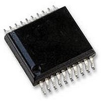
BD4154FV-E2 Rohm Semiconductor, BD4154FV-E2 Datasheet - Page 7

BD4154FV-E2
Manufacturer Part Number
BD4154FV-E2
Description
POWER SWITCH EXPRESS CARD, SSOP-B20
Manufacturer
Rohm Semiconductor
Series
-r
Specifications of BD4154FV-E2
Primary Input Voltage
3.6V
No. Of Outputs
1
Output Voltage
5V
Output Current
1.3A
Voltage Regulator Case Style
SSOP
No. Of Pins
20
Operating Temperature Range
-40°C To +100°C
Svhc
No SVHC
Applications
PCMCIA, ExpressCard™
Current - Supply
250µA
Voltage - Supply
3 V ~ 3.6 V
Operating Temperature
-40°C ~ 100°C
Mounting Type
Surface Mount
Package / Case
20-TSSOP (0.173", 4.40mm Width)
Lead Free Status / RoHS Status
Lead free / RoHS Compliant
●Description of block operation
BD4154FV
© 2010 ROHM Co., Ltd. All rights reserved.
www.rohm.com
EN
V3_IN, V15_IN, and V3AUX_IN
V3, V15, and V3AUX
CPPE#
CPUSB#
SYSR
PERST_IN#
PERST#
RCLKEN
TEST
With an input of 2.0 volts or higher, this terminal goes HIGH to activate the circuit, and goes LOW to deactivate the circuit
(with the standby circuit current of 40 μA), It discharges each output and lowers output voltage when the input falls to 0.8
volts or less.
These are the input terminals for each channel of a 3ch switch. V3_IN and V15_IN terminals have two pins each, which
should be short-circuited on the pc board with a thick conductor. A large current runs through these three terminals :
(V3_IN: 1.35A; V3AUX_IN: 0.275 A; and V15_IN: 0.625 A). In order to lower the output impedance of the connected power
supply, it is recommended that ceramic capacitors (with B-type characteristics or better) be provided between these
terminals and the ground. Specifically, the capacitors should be on the order of 1 μF between V3_IN and GND, and between
V15_IN and GND; and on the order of 0.1 μF between V3AUX_IN and GND.
These are the output terminals for each switch.
short-circuited on the PC board and connected to an ExpressCard connector with a thick conductor, as short as possible.
In order to stabilize the output, it is recommended that ceramic capacitors (with B-type characteristics or better) be provided
between these terminals and the ground. Specifically, the capacitors should be on the order of 10 μF between V3 and GND,
and between V15 and GND; and on the order of 1 μF between V3AUX and GND.
This pin is used to find whether or not a PCI-Express signal compatible card is present. Turns to “High” level with an input
of 2.0 volts or higher, which means that no card is provided, while it turns to “Low” level when the input is lowered to 0.8 volts
or less, which means that a card is provided. Controls the ON/OFF, switch selecting the proper mode based on the status
of the system.
Pull up resistance (100kΩ~200kΩ) is built into, so the number of components is reduced.
This pin is used to find whether or not a USB2.0 signal compatible card is present. Turns to “High” level with an input of 2.0
volts or higher, which means that no card is provided, while it turns to “Low” level when the input is lowered to 0.8 volts or
less, which means that a card is provided. Controls the ON/OFF switch, selecting the proper mode based on the system
status.
Pull up resistance (100kΩ~200kΩ) is built into, so the number of components is reduced.
This pin is used to detect the system status. Turns to “High” level with an input of 2.0 volts or higher, which means that the
system is activated, while it turns to “Low” level when the input is lowered to 0.8 volts or less, which means that the system is
on standby.
This pin is used to control the reset signal (PERST#) to a card from the system side. (Also referred to as “SysReset#” by
PCMCIA.) Turns to “High” level with an input of 2.0 volts or higher, and sets PERST# to “High” AND with a “Power Good”
output. Turns to “Low” level and sets PERST# to “Low” when the input falls to 0.8 volts or less.
This pin is used to send a reset signal to a PCI-Express compatible card. Reset status is determined by the outputs,
PERST_IN#, CPPE# system status, and EN on/off status. Turns to “High” level and activates the PCI-Express compatible
card only if each output is within the “Power Good” threshold, with the card inserted and PERST_IN# turned to “High” level.
This pin is used to send an enable signal to the reference clock. Activation status is determined by the outputs, CPPE#
system status, and EN on/off status. Turns to “High” level and activates the reference clock PLL only if each output is within
the “Power Good” threshold, with the card kept inserted.
This pin is used to test, which should be short-circuited to the GND. When it is short-circuited to V3AUX_IN, UVLO (V3_IN,
V15_IN) turns OFF.
The V3 and V15 terminals have two pins each, which should be
7/15
Technical Note
2010.04 - Rev.B


