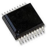
BD4154FV-E2 Rohm Semiconductor, BD4154FV-E2 Datasheet

BD4154FV-E2
Specifications of BD4154FV-E2
Related parts for BD4154FV-E2
BD4154FV-E2 Summary of contents
Page 1
... ExpressCard BD4154FV ●Description BD4154FV is a power management switch IC for the next generation PC card (ExpressCard It conforms to the PCMCIA ExpressCard Guideline, and obtains the Compliance ID “EC100040” from PCMCIA. The power switch offers a number of functions - card detector, and system status detector - which are ideally suited for laptop and desktop computers. ...
Page 2
... BD4154FV ●Absolute Maximum Ratings Parameter Input Voltage Logic Input Voltage 1 Logic Output Voltage 1 Logic Output Voltage 2 Output Voltage Output Current 1 Output Current 2 Output Current 3 Power Dissipation 1 Power Dissipation 2 Operating Temperature Range Storage Temperature Range Maximum Junction Temperature *1 Not to exceed Pd. *2 Reduced by 4.0mW for each increase 1℃ over 25℃ ...
Page 3
... BD4154FV ●Electrical Characteristics (unless otherwise noted, Ta=25℃ VEN=3.3V V3AUX_IN =V3_IN=3.3V,V15_IN=1.5V) Parameter Standby Current Bias Current 1 Bias Current 2 [Enable] High Level Enable Input Voltage Low Level Enable Input Voltage Enable Pin Input Current [Logic] High Level Logic Input Voltage Low Level Logic Input Voltage ...
Page 4
... BD4154FV ●Reference data CPPE#(2V/div) V3(2V/div) V3AUX(2V/div) V15(1V/div) 5.0ms/div Fig.1 Card Assert/ De-assert (Active) SYSR(2V/div) V3(2V/div) V3AUX(2V/div) V15(1V/div) 5.0ms/div Fig.4 System Active⇔Standby (No Card) EN(2V/div) V3(2V/div) V3AUX(2V/div) V15(1V/div) 500μs/div Fig.7 Wakeup Wave Form (Shut Down→Active) CPUSB#(2V/div) V3(2V/div) V3AUX(2V/div) V15(1V/div) 500µ ...
Page 5
... BD4154FV CPPE#(2V/div) V3(2V/div) V3AUX(2V/div) PERST#(2V/div) 5.0ms/div Fig.13 PERST# Wave Form (Card Assert/ De-assert) CPUSB#(2V/div) V3(2V/div) V3AUX(2V/div) RCLKEN(2V/div) 5.0ms/div Fig.16 RCLKEN Wave Form (USB2.0 Assert/ De-assert) V3_IN(2V/div) V3(2V/div) V3AUX(2V/div) V15(1V/div) 500μs/div Fig.19 Output Voltage (V3_IN:OFF→ON) V3_IN(2V/div) V3(2V/div) ...
Page 6
... BD4154FV ●Block Diagram V3_IN1 4 5 3.3V V3_IN2 V3AUX_IN 18 3.3V V15_IN1 15 V15_IN2 1.5V 16 CPPE# 12 CPUSB# 11 SYSR 3 V3AUX_IN EN 2 ●PIN CONFIGRATION PERST_IN SYSR 3 V3_IN1 4 V3_IN2 5 V3_1 6 V3_2 7 PERST TEST 10 GND SSOP-B20 Package www.rohm.com © 2010 ROHM Co., Ltd. All rights reserved. VD TSD,CL,UVLO VD TSD,CL,UVLO_AUX VD Input ...
Page 7
... BD4154FV ●Description of block operation EN With an input of 2.0 volts or higher, this terminal goes HIGH to activate the circuit, and goes LOW to deactivate the circuit (with the standby circuit current of 40 μA), It discharges each output and lowers output voltage when the input falls to 0.8 volts or less ...
Page 8
... BD4154FV ●Timing Chart System Status ExpressCard Primary Auxiliary OFF OFF SYSR=H⇔L CP#=H SYSR=L CP#=H⇔L V3AUX=OFF V15=V3=OFF SYSR=H SYSR=L ⇔ CP#=L System Status Stand-by Status ON Status From ON to Stand-by Status From Stand- Status www.rohm.com © 2010 ROHM Co., Ltd. All rights reserved. ...
Page 9
... GND SW2 PERST_IN GND GND SW3 GND GND SYSR C3 GND V3_IN C4 GND V3 C6 GND PERST # V3AUX_IN SW7 GND BD4154FV Evaluation Board Application Components ■ ■ Part No Value R1 0Ω R2 0Ω R3 0Ω R11 0Ω R12 0Ω 1μF C6 10μF C11 ...
Page 10
... BD4154FV BD4154FV Evaluation Board Layout ■ ■ Silk Screen Mid Layer 1 Bottom Layer www.rohm.com © 2010 ROHM Co., Ltd. All rights reserved. TOP Layer Mid Layer 2 10/15 Technical Note 2010.04 - Rev.B ...
Page 11
... Single-layer substrate (substrate surface copper foil area: less than 3%) Most of heat loss in the BD4154FV occurs at the output switch. The power lost is determined by multiplying the on-resistance by the square of output current of each switch. www.rohm.com © 2010 ROHM Co., Ltd. All rights reserved. ...
Page 12
... BD4154FV ●Equivalent Circuit 1pin<PERST_IN#> V3AUX_IN V3AUX_IN 4,5pin<V3_IN1,V3_IN2> V3 9pin<TEST> 13,14pin<V15_1,V15_2> V3_IN 18pin<V3AUX_IN> V3AUX www.rohm.com © 2010 ROHM Co., Ltd. All rights reserved. 2pin<EN> V3AUX_IN V3AUX_IN 6,7pin<V3_1,V3_2> V3_IN 11pin<CPUSB#> V3AUX_IN V3AUX_IN 15,16pin<V15_IN1,V15_IN2> V15 19pin<RCLKEN > V3AUX_IN 12/15 Technical Note 3pin<SYSR> V3AUX_IN V3AUX_IN 8pin<PERST#> V3AUX_IN 12pin<CPPE#> ...
Page 13
... BD4154FV ●Notes for Use 1.Absolute maximum ratings Although quality is rigorously controlled, the device may be destroyed when applied voltage, operating temperature, etc. exceeds its absolute maximum rating. Because the source (short mode or open mode) cannot be identified once the IC is destroyed important to take physical safety measures such as fusing when implementing any special mode that operates in excess of absolute rating limits ...
Page 14
... BD4154FV 10. Electrical characteristics The electrical characteristics in the Specifications may vary, depending on ambient temperature, power supply voltage, circuit(s) externally applied, and/or other conditions. characteristics, that could affect the electrical characteristics. 11. Capacitors applied to input terminals The capacitors applied to the input terminals (V3_IN, V3AUX_IN and V15_IN) are used to lower the output impedance of the connected power supply ...
Page 15
... BD4154FV ●Ordering part number Part Number Part Number SSOP-B20 6.5 ± 0 0.1 0.65 0.22 ± 0.1 www.rohm.com © 2010 ROHM Co., Ltd. All rights reserved Package FV : SSOP-B20 <Tape and Reel information> Tape Embossed carrier tape Quantity 2500pcs E2 Direction The direction is the 1pin of product is at the upper left when you hold ...
Page 16
No copying or reproduction of this document, in part or in whole, is permitted without the consent of ROHM Co.,Ltd. The content specified herein is subject to change for improvement without notice. The content specified herein is for the purpose ...


