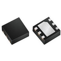
LT3493EDCB#PBF Linear Technology, LT3493EDCB#PBF Datasheet - Page 8

LT3493EDCB#PBF
Manufacturer Part Number
LT3493EDCB#PBF
Description
IC, STEP-DOWN PWM DC/DC CONVERTER, DFN-6
Manufacturer
Linear Technology
Datasheet
1.LT3493EDCBTRMPBF.pdf
(20 pages)
Specifications of LT3493EDCB#PBF
Primary Input Voltage
36V
No. Of Outputs
1
Output Current
1.2A
No. Of Pins
6
Operating Temperature Range
-40°C To +85°C
Supply Voltage Range
3.6V To 36V
Switching Frequency Max
815kHz
Msl
MSL 1 - Unlimited
Rohs Compliant
Yes
Lead Free Status / RoHS Status
Lead free / RoHS Compliant
Available stocks
Company
Part Number
Manufacturer
Quantity
Price
LT3493
APPLICATIONS INFORMATION
FB Resistor Network
The output voltage is programmed with a resistor divider
between the output and the FB pin. Choose the 1% resis-
tors according to:
R2 should be 20k or less to avoid bias current errors.
Reference designators refer to the Block Diagram.
An optional phase lead capacitor of 22pF between V
and FB reduces light-load output ripple.
Input Voltage Range
The input voltage range for LT3493 applications depends
on the output voltage and on the absolute maximum rat-
ings of the V
The minimum input voltage is determined by either the
LT3493’s minimum operating voltage of 3.6V, or by its
maximum duty cycle. The duty cycle is the fraction of
time that the internal switch is on and is determined by
the input and output voltages:
where V
(~0.4V) and V
(~0.4V at maximum load). This leads to a minimum input
voltage of:
with DC
The maximum input voltage is determined by the absolute
maximum ratings of the V
tinuous mode operation, the maximum input voltage is
determined by the minimum duty cycle DC
Note that this is a restriction on the operating input voltage
for continuous mode operation; the circuit will tolerate
transient inputs up to the absolute maximum ratings
8
R1= R2
DC =
V
V
IN(MIN)
IN(MAX)
MAX
D
V
IN
is the forward voltage drop of the catch diode
V
=
0.78V
OUT
– V
= 0.91 (0.88 over temperature).
IN
=
V
SW
OUT
V
V
and BOOST pins.
SW
OUT
DC
OUT
+ V
DC
is the voltage drop of the internal switch
MAX
+ V
– 1
D
MIN
+ V
+ V
D
D
D
– V
– V
IN
D
and BOOST pins. For con-
D
+ V
+ V
SW
SW
MIN
= 0.10:
OUT
of the V
limited to the V
conditions (short-circuit or start-up).
Minimum On Time
The part will still regulate the output at input voltages that
exceed V
ripple increases as the input voltage is increased. Figure 1
illustrates switching waveforms in continuous mode for a
3V output application near V
As the input voltage is increased, the part is required
to switch for shorter periods of time. Delays associated
with turning off the power switch dictate the minimum
on time of the part. The minimum on time for the LT3493
is ~120ns. Figure 2 illustrates the switching waveforms
when the input voltage is increased to V
AC COUPLED
AC COUPLED
200mV/DIV
200mV/DIV
0.5A/DIV
0.5A/DIV
20V/DIV
20V/DIV
V
V
V
V
OUT
OUT
IN
SW
SW
IN(MAX)
I
I
L
L
and BOOST pins. The input voltage should be
C
V
V
I
L = 10μH
C
V
V
I
L = 10μH
LOAD
LOAD
OUT
OUT
IN
OUT
OUT
IN
= 30V
= 35V
= 10μF
= 3V
= 10μF
= 3V
= 0.75A
= 0.75A
IN
(up to 40V), however, the output voltage
operating range (36V) during overload
Figure 1
Figure 2
2μs/DIV
2μs/DIV
IN(MAX)
= 33V.
IN
= 35V.
3493 F02
3493 F01
3493fb


