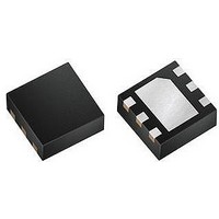
LT3493EDCB#PBF Linear Technology, LT3493EDCB#PBF Datasheet - Page 17

LT3493EDCB#PBF
Manufacturer Part Number
LT3493EDCB#PBF
Description
IC, STEP-DOWN PWM DC/DC CONVERTER, DFN-6
Manufacturer
Linear Technology
Datasheet
1.LT3493EDCBTRMPBF.pdf
(20 pages)
Specifications of LT3493EDCB#PBF
Primary Input Voltage
36V
No. Of Outputs
1
Output Current
1.2A
No. Of Pins
6
Operating Temperature Range
-40°C To +85°C
Supply Voltage Range
3.6V To 36V
Switching Frequency Max
815kHz
Msl
MSL 1 - Unlimited
Rohs Compliant
Yes
Lead Free Status / RoHS Status
Lead free / RoHS Compliant
Available stocks
Company
Part Number
Manufacturer
Quantity
Price
APPLICATIONS INFORMATION
High Temperature Considerations
The die temperature of the LT3493 must be lower than the
maximum rating of 125°C. This is generally not a concern
unless the ambient temperature is above 85°C. For higher
temperatures, care should be taken in the layout of the
circuit to ensure good heat sinking of the LT3493. The
maximum load current should be derated as the ambient
temperature approaches 125°C. The die temperature is
calculated by multiplying the LT3493 power dissipation by
the thermal resistance from junction to ambient. Power
dissipation within the LT3493 can be estimated by calcu-
lating the total power loss from an effi ciency measure-
ment and subtracting the catch diode loss. The resulting
temperature rise at full load is nearly independent of input
voltage. Thermal resistance depends on the layout of the
circuit board, but 64°C/W is typical for the (2mm × 3mm)
DFN (DCB) package.
TYPICAL APPLICATIONS
3.6V TO 25V
3.6V TO 25V
ON OFF
ON OFF
V
V
IN
IN
2.2μF
2.2μF
V
SHDN
V
SHDN
IN
IN
0.78V Step-Down Converter
1.8V Step-Down Converter
LT3493
LT3493
1N4148
GND
1N4148
GND
BOOST
BOOST
SW
SW
FB
FB
Outputs Greater Than 6V
For outputs greater than 6V, add a resistor of 1k to 2.5k
across the inductor to damp the discontinuous ringing
of the SW node, preventing unintended SW current. The
12V Step-Down Converter circuit in the Typical Applica-
tions section shows the location of this resistor. Also note
that for outputs above 6V, the input voltage range will be
limited by the maximum rating of the BOOST pin. The 12V
circuit shows how to overcome this limitation using an
additional zener diode.
Other Linear Technology Publications
Application notes AN19, AN35 and AN44 contain more
detailed descriptions and design information for Buck
regulators and other switching regulators. The LT1376
data sheet has a more extensive discussion of output
ripple, loop compensation and stability testing. Design
Note DN100 shows how to generate a bipolar output
supply using a Buck regulator.
0.1μF 3.3μH
MBRM140
0.1μF
MBRM140
5μH
26.1k
20k
3493 TA02
3493 TA03
47μF
22μF
V
0.78V
1.2A
V
1.8V
1.2A
OUT
OUT
LT3493
17
3493fb


