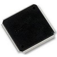
LPC2212FBD144 NXP Semiconductors, LPC2212FBD144 Datasheet - Page 10

LPC2212FBD144
Manufacturer Part Number
LPC2212FBD144
Description
16/32BIT MCU ARM7, 128K FLASH, 144LQFP
Manufacturer
NXP Semiconductors
Datasheet
1.LPC2212FBD144.pdf
(45 pages)
Specifications of LPC2212FBD144
No. Of I/o's
112
Ram Memory Size
16KB
Cpu Speed
60MHz
No. Of Timers
2
No. Of Pwm Channels
6
Digital Ic Case
RoHS Compliant
Core Size
32bit
Program Memory Size
128KB
Oscillator Type
External Only
Controller Family/series
LPC22xx
Rohs Compliant
Yes
Available stocks
Company
Part Number
Manufacturer
Quantity
Price
Company:
Part Number:
LPC2212FBD144,551
Manufacturer:
NXP Semiconductors
Quantity:
10 000
Company:
Part Number:
LPC2212FBD144/01,5
Manufacturer:
NXP Semiconductors
Quantity:
10 000
NXP Semiconductors
Table 3.
LPC2212_2214_4
Product data sheet
Symbol
P3[3]/A3
P3[4]/A4
P3[5]/A5
P3[6]/A6
P3[7]/A7
P3[8]/A8
P3[9]/A9
P3[10]/A10
P3[11]/A11
P3[12]/A12
P3[13]/A13
P3[14]/A14
P3[15]/A15
P3[16]/A16
P3[17]/A17
P3[18]/A18
P3[19]/A19
P3[20]/A20
P3[21]/A21
P3[22]/A22
P3[23]/A23/XCLK
P3[24]/CS3
P3[25]/CS2
P3[26]/CS1
P3[27]/WE
P3[28]/BLS3/AIN7
P3[29]/BLS2/AIN6
P3[30]/BLS1
P3[31]/BLS0
n.c.
RESET
XTAL1
XTAL2
Pin description
Pin
81
80
74
73
72
71
66
65
64
63
62
56
55
53
48
47
46
45
44
41
40
36
35
30
29
28
27
97
96
22
135
142
141
…continued
Type Description
O
O
O
O
O
O
O
O
O
O
O
O
O
O
O
O
O
O
O
O
O
O
O
O
O
O
O
I
O
I
O
O
I
I
O
External memory address line 3.
External memory address line 4.
External memory address line 5.
External memory address line 6.
External memory address line 7.
External memory address line 8.
External memory address line 9.
External memory address line 10.
External memory address line 11.
External memory address line 12.
External memory address line 13.
External memory address line 14.
External memory address line 15.
External memory address line 16.
External memory address line 17.
External memory address line 18.
External memory address line 19.
External memory address line 20.
External memory address line 21.
External memory address line 22.
A23 — External memory address line 23.
XCLK — Clock output.
LOW-active Chip Select 3 signal.
(Bank 3 addresses range 0x8300 0000 to 0x83FF FFFF)
LOW-active Chip Select 2 signal.
(Bank 2 addresses range 0x8200 0000 to 0x82FF FFFF)
LOW-active Chip Select 1 signal.
(Bank 1 addresses range 0x8100 0000 to 0x81FF FFFF)
LOW-active Write enable signal.
BLS3 — LOW-active Byte Lane Select signal (Bank 3).
AIN7 — ADC, input 7. This analog input is always connected to its pin.
BLS2 — LOW-active Byte Lane Select signal (Bank 2).
AIN6 — ADC, input 6. This analog input is always connected to its pin.
LOW-active Byte Lane Select signal (Bank 1).
LOW-active Byte Lane Select signal (Bank 0).
Pin not connected.
external reset input; a LOW on this pin resets the device, causing I/O ports
and peripherals to take on their default states, and processor execution to
begin at address 0. TTL with hysteresis, 5 V tolerant.
input to the oscillator circuit and internal clock generator circuits.
output from the oscillator amplifier.
Rev. 04 — 3 January 2008
16/32-bit ARM microcontrollers
LPC2212/2214
© NXP B.V. 2008. All rights reserved.
10 of 45


