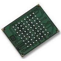
S29GL128P10FFI010 Spansion Inc., S29GL128P10FFI010 Datasheet - Page 67

S29GL128P10FFI010
Manufacturer Part Number
S29GL128P10FFI010
Description
IC, FLASH, 128MBIT, 100NS, BGA-64
Manufacturer
Spansion Inc.
Datasheet
1.S29GL128P10FFI010.pdf
(80 pages)
Specifications of S29GL128P10FFI010
Memory Type
Flash
Memory Size
128Mbit
Memory Configuration
16M X 8 / 8M X 16
Ic Interface Type
CFI, Parallel
Access Time
100ns
Supply Voltage Range
2.7 To 3.6 V
Memory Case Style
BGA
Cell Type
NOR
Density
128Mb
Access Time (max)
100ns
Interface Type
Parallel
Boot Type
Not Required
Address Bus
24/23Bit
Operating Supply Voltage (typ)
3/3.3V
Operating Temp Range
-40C to 85C
Package Type
Fortified BGA
Sync/async
Asynchronous
Operating Temperature Classification
Industrial
Operating Supply Voltage (min)
2.7V
Operating Supply Voltage (max)
3.6V
Word Size
8/16Bit
Number Of Words
16M/8M
Supply Current
110mA
Mounting
Surface Mount
Pin Count
64
Rohs Compliant
Yes
Lead Free Status / RoHS Status
Lead free / RoHS Compliant
Available stocks
Company
Part Number
Manufacturer
Quantity
Price
Company:
Part Number:
S29GL128P10FFI010
Manufacturer:
XILINX
Quantity:
364
Part Number:
S29GL128P10FFI010
Manufacturer:
SPANSION
Quantity:
20 000
Company:
Part Number:
S29GL128P10FFI010A
Manufacturer:
SPANSION
Quantity:
10 393
Notes
1. Typical program and erase times assume the following conditions: 25°C, 3.6 V V
2. Under worst case conditions of -40°C, V
3. Effective write buffer specification is based upon a 32-word write buffer operation.
4. In the pre-programming step of the Embedded Erase algorithm, all bits are programmed to 00h before erasure.
5. System-level overhead is the time required to execute the two- or four-bus-cycle sequence for the program command. See Tables 12.1–12.4.
November 17, 2010 S29GL-P_00_A13
Sector Erase Time
Chip Erase Time
Total Write Buffer Time
Total Accelerated Write Buffer Programming Time
(Note 3)
Chip Program Time
11.7.5
11.7.6
Erase And Programming Performance
TSOP Pin and BGA Package Capacitance
Notes
1. Sampled, not 100% tested.
2. Test conditions T
Parameter
Parameter Symbol
(Note 3)
WP#/ACC
RESET#
C
C
CE#
C
OUT
IN2
IN
CC
A
S29GL01GP
S29GL01GP
S29GL128P
S29GL256P
S29GL512P
S29GL128P
S29GL256P
S29GL512P
= 25°C, f = 100 MHz.
= 3.0 V, 100,000 cycles.
Table 11.8 Erase And Programming Performance
D a t a
S29GL-P MirrorBit
Control Pin Capacitance
Parameter Description
Separated Control Pin
Separated Control Pin
Separated Control Pin
Output Capacitance
Input Capacitance
S h e e t
Table 11.9 Package Capacitance
(Note 1)
Typ
128
256
512
480
432
123
246
492
984
0.5
64
CC
®
Flash Family
, 10,000 cycles, checkerboard pattern.
(Note 2)
1024
2048
Max
256
512
3.5
Test Setup
V
V
V
V
V
V
OUT
IN
IN
IN
IN
IN
= 0
= 0
= 0
= 0
= 0
= 0
Unit
sec
sec
sec
µs
µs
Excludes 00h programming
prior to erasure
Excludes system level
overhead
Typ
10
42
25
22
6
8
Comments
(Note 5)
Max
10
12
10
45
28
25
(Note 4)
Unit
pF
pF
pF
pF
pF
pF
67


