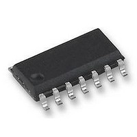
74HC02D NXP Semiconductors, 74HC02D Datasheet - Page 6

74HC02D
Manufacturer Part Number
74HC02D
Description
IC, 74HC CMOS, SMD, 74HC02, SOIC14
Manufacturer
NXP Semiconductors
Datasheet
1.74HC02D653.pdf
(15 pages)
Specifications of 74HC02D
Output Current
5.2mA
No. Of Inputs
2
Supply Voltage Range
2V To 6V
Logic Case Style
SOIC
No. Of Pins
14
Operating Temperature Range
-40°C To +125°C
Svhc
No SVHC
Logic Type
NOR Gate
Lead Free Status / RoHS Status
Lead free / RoHS Compliant
Available stocks
Company
Part Number
Manufacturer
Quantity
Price
Company:
Part Number:
74HC02D
Manufacturer:
NXP
Quantity:
17 600
Company:
Part Number:
74HC02D
Manufacturer:
PHILIPS
Quantity:
59 190
Company:
Part Number:
74HC02D
Manufacturer:
NXP
Quantity:
2 380
Part Number:
74HC02D
Manufacturer:
NXP/恩智浦
Quantity:
20 000
Company:
Part Number:
74HC02D,653
Manufacturer:
NXP
Quantity:
10 000
Part Number:
74HC02DB
Manufacturer:
PHILIPS/飞利浦
Quantity:
20 000
NXP Semiconductors
Table 7.
GND = 0 V; C
[1]
[2]
[3]
11. Waveforms
Table 8.
74HC_HCT02_3
Product data sheet
Symbol Parameter
74HCT02
t
t
C
Type
74HC02
74HCT02
pd
t
Fig 6.
PD
t
t
C
P
f
f
C
V
N = number of inputs switching;
pd
t
i
o
D
CC
is the same as t
PD
L
= output frequency in MHz;
= input frequency in MHz;
(C
is the same as t
= output load capacitance in pF;
= C
is used to determine the dynamic power dissipation (P
= supply voltage in V;
L
propagation delay nA, nB to nY; see
transition time
power dissipation
capacitance
Measurement points are given in
V
Input to output propagation delays
PD
V
OL
Dynamic characteristics
Measurement points
CC
L
and V
V
2
= 50 pF; for load circuit see
CC
f
2
o
) = sum of outputs.
OH
THL
PHL
f
i
are typical voltage output levels that occur with the output load.
and t
N +
and t
Input
V
0.5V
1.3 V
M
TLH
PLH
CC
(C
Conditions
V
per package;
V
.
CC
I
.
L
V
V
= GND to V
nA, nB input
CC
CC
= 4.5 V; see
V
nY output
CC
= 4.5 V
= 5.0 V; C
2
Table
GND
V
V
f
o
OH
OL
Figure
V
) where:
I
CC
9.
L
Figure 6
Rev. 03 — 18 September 2008
Figure 6
= 15 pF
1.5 V
7.
Output
V
0.5V
1.3 V
V
M
M
t
t
THL
PHL
CC
V
D
Y
in W):
V
M
V
X
[1]
[2]
[3]
Min
t
TLH
-
-
-
-
t
PLH
V
0.1V
0.1V
X
25 C
CC
CC
Typ
11
24
74HC02; 74HCT02
9
7
001aai814
Max
19
15
-
-
Quad 2-input NOR gate
(85 C)
40 C to +125 C Unit
Max
24
19
V
0.9V
0.9V
-
-
Y
© NXP B.V. 2008. All rights reserved.
CC
CC
(125 C)
Max
29
22
-
-
ns
ns
ns
pF
6 of 15


