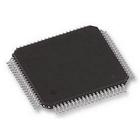
SC16C554BIB80 NXP Semiconductors, SC16C554BIB80 Datasheet - Page 17

SC16C554BIB80
Manufacturer Part Number
SC16C554BIB80
Description
IC, UART, QUAD, 16BYTE FIFO, 16C554
Manufacturer
NXP Semiconductors
Datasheet
1.SC16C554BIB80528.pdf
(58 pages)
Specifications of SC16C554BIB80
No. Of Channels
4
Data Rate
5Mbps
Supply Voltage Range
2.25V To 5.5V
Operating Temperature Range
-40°C To +85°C
Digital Ic Case Style
LQFP
No. Of Pins
80
Svhc
No SVHC (18-Jun-2010)
Uart Features
Pin & Software Compatible, 16-Byte Transmit FIFO, Automatic Hardware Flow Control
Rohs Compliant
Yes
Lead Free Status / RoHS Status
Lead free / RoHS Compliant
Available stocks
Company
Part Number
Manufacturer
Quantity
Price
Company:
Part Number:
SC16C554BIB80
Manufacturer:
NXP
Quantity:
1 000
Part Number:
SC16C554BIB80
Manufacturer:
NXP/恩智浦
Quantity:
20 000
Company:
Part Number:
SC16C554BIB80,528
Manufacturer:
Maxim
Quantity:
278
Company:
Part Number:
SC16C554BIB80,528
Manufacturer:
NXP Semiconductors
Quantity:
10 000
NXP Semiconductors
SC16C554B_554DB
Product data sheet
6.2 Internal registers
6.3 FIFO operation
The SC16C554B/554DB provides 12 internal registers for monitoring and control. These
registers are shown in
(THR/RHR), interrupt status and control registers (IER/ISR), a FIFO Control Register
(FCR), line status and control registers (LCR/LSR), modem status and control registers
(MCR/MSR), programmable data rate (clock) control registers (DLL/DLM), and a user
accessible Scratchpad Register (SPR). Register functions are more fully described in the
following paragraphs.
Table 5.
[1]
[2]
The 16 byte transmit and receive data FIFOs are enabled by the FIFO Control Register
(FCR) bit 0. With SC16C554B devices, the user can set the receive trigger level, but not
the transmit trigger level. The receiver FIFO section includes a time-out function to ensure
data is delivered to the external CPU. An interrupt is generated whenever the Receive
Holding Register (RHR) has not been read following the loading of a character or the
receive trigger level has not been reached.
Table 6.
A2
General register set (THR/RHR, IER/ISR, MCR/MSR, FCR, LCR/LSR, SPR)
0
0
0
0
1
1
1
1
Baud rate register set (DLL/DLM)
0
0
Selected trigger level
(characters)
1
4
8
14
These registers are accessible only when LCR[7] is a logic 0.
These registers are accessible only when LCR[7] is a logic 1.
A1
0
0
1
1
0
0
1
1
0
0
Internal registers decoding
Flow control mechanism
A0
0
1
0
1
0
1
0
1
0
1
All information provided in this document is subject to legal disclaimers.
5 V, 3.3 V and 2.5 V quad UART, 5 Mbit/s (max.) with 16-byte FIFOs
Table
Read mode
Receive Holding Register
Interrupt Enable Register
Interrupt Status Register
Line Control Register
Modem Control Register
Line Status Register
Modem Status Register
Scratchpad Register
LSB of Divisor Latch
MSB of Divisor Latch
Rev. 4 — 8 June 2010
5. These registers function as data holding registers
INTn pin activation
1
4
8
14
[2]
SC16C554B/554DB
Negate RTS
4
8
12
14
Write mode
Transmit Holding Register
Interrupt Enable Register
FIFO Control Register
Line Control Register
Modem Control Register
n/a
n/a
Scratchpad Register
LSB of Divisor Latch
MSB of Divisor Latch
[1]
© NXP B.V. 2010. All rights reserved.
Assert RTS
1
4
8
10
17 of 58


