TB6562AFG Toshiba, TB6562AFG Datasheet
TB6562AFG
Specifications of TB6562AFG
Available stocks


Related parts for TB6562AFG

TB6562AFG Summary of contents
Page 1
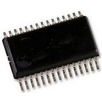
... Ensure also that the ambient temperature and relative humidity are maintained at reasonable levels. Special care should be taken with the following pins, which are vulnerable to surge current. Pins with low surge withstand capability: TB6562ANG: pins 10, 15 TB6562AFG: pins 13, 18 TB6562ANG/AFG TB6562ANG TB6562AFG SSOP30-P-375-1.00 Weight: SDIP24-P-300-1 ...
Page 2
... Some functional blocks, circuits, or constants may be omitted or simplified in the block diagram for explanatory purposes. < TB6562ANG > GND Vreg SB OSC OSC 5 V Waveform squaring Thermal shutdown Control logic Decoder GND Phase A X1A X2A < TB6562AFG > GND Vreg SB OSC OSC 5 V Waveform squaring Thermal shutdown Control logic Decoder GND Phase A X1A X2A V ...
Page 3
... Connect to a motor coil pin. Vcc (opr Apply signal, Built-in pull down resistance of 100kΩ(typ.) Apply signal, Built-in pull down resistance of 100kΩ(typ.) Apply signal, Built-in pull down resistance of 100kΩ(typ (opr) TB6562AFG 1 30 GND 2 29 Vreg 3 28 ...
Page 4
... TB6562AFG > Pin No. Symbol 1 GND Ground pin 2 Vreg 5 V output pin 3 SB Standby pin 4 Phase A Rotation direction control pin (Ch X1A Input pin used to set output current level (Ch X2A Input pin used to set output current level (Ch GND Ground pin 8 GND Ground pin ...
Page 5
Absolute Maximum Ratings Characteristic Power supply voltage Output voltage Output current Input voltage Power dissipation Operating temperature Storage temperature Junction temperature Note 1: Output current may be controlled by excitation mode, ambient temperature, or heatsink. When designing a circuit, ensure ...
Page 6
Electrical Characteristics Characteristic Supply current Input voltage Control circuit Input hysteresis voltage (Note 1) Input current Input voltage Input hysteresis Standby circuit voltage Input current Output ON-resistance Output leakage current Diode forward voltage Internal reference voltage Input current Vref circuit ...
Page 7
Truth Tables < 2-phase excitation > (*) Io: OUT1 → OUT2; + current Phase A Input Phase A X1A X2A < 1–2-phase excitation > Phase A Input Phase ...
Page 8
Timing Charts Timing charts may be simplified for explanatory < 2-phase excitation > 100% I (A) O −100% 100% I (B) O −100% H Phase X1A L H X2A L H Phase X1B L ...
Page 9
W 1–2-phase excitation > 100% 66.7% 33. −33.3% −66.7% −100% 100% 66.7% 33. −33.3% −66.7% −100% H Phase X1A L H X2A L H Phase ...
Page 10
PWM Current Control The IC enters CW (CCW) mode and short brake mode alternately during PWM current control. To prevent shoot-through current caused by simultaneous conduction of upper and lower transistors in the output stage, a dead time is internally ...
Page 11
Constant current regulation When V reaches the reference voltage (Vref), the IC enters discharge mode. After four clock signals are RS generated from the oscillator, the IC moves from discharge mode to charge mode. Vref OSC Internal clock Vref V ...
Page 12
Transition from charge mode to discharge mode > Vref after four clock signals in charge mode, the IC again enters discharge mode. After a further four clock signals in discharge mode, V mode until V reaches Vref. ...
Page 13
Reference Voltage Generator The current value at 100% is determined by applying voltage at the Vref pin. The value can be calculated as follows: OUT1 Thermal Shutdown Circuit (TSD) The IC incorporates a thermal ...
Page 14
... Application Circuit The application circuit below is for reference only and requires thorough evaluation at the mass production design stage. In furnishing this example of an application circuit, Toshiba does not grant the use of any industrial property rights PORT1 PORT2 PORT3 PORT4 PORT5 PORT6 PORT7 ...
Page 15
Package Dimensions Weight: 1.62 g (typ.) TB6562ANG/AFG 15 2007-3-22 ...
Page 16
Weight: 0.63 g (typ.) TB6562ANG/AFG 16 2007-3-22 ...
Page 17
... Application Circuits The application circuits shown in this document are provided for reference purposes only. Thorough evaluation is required, especially at the mass production design stage. Toshiba does not grant any license to any industrial property rights by providing these examples of application circuits. 5. Test Circuits Components in the test circuits are used only to obtain and confirm the device characteristics. These components and circuits are not guaranteed to prevent malfunction or failure from occurring in the application equipment ...
Page 18
Points to remember on handling of ICs (1) Over current Protection Circuit Over current protection circuits (referred to as current limiter circuits) do not necessarily protect ICs under all circumstances. If the Over current protection circuits operate against the over ...
Page 19
... The information contained herein is presented only as a guide for the applications of our products. No responsibility is assumed by TOSHIBA for any infringements of patents or other rights of the third parties which may result from its use. No license is granted by implication or otherwise under any patents or other rights of TOSHIBA or the third parties ...