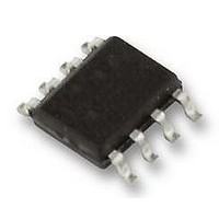
LM27222M National Semiconductor, LM27222M Datasheet - Page 5

LM27222M
Manufacturer Part Number
LM27222M
Description
MOSFET DRIVER/PWM CONTROL, 27222
Manufacturer
National Semiconductor
Datasheet
1.LM27222M.pdf
(11 pages)
Specifications of LM27222M
Device Type
MOSFET
Module Configuration
High Side / Low Side
Peak Output Current
4.5A
Output Resistance
10kohm
Supply Voltage Range
4V To 7V
Driver Case Style
SOIC
No. Of Pins
8
Operating
RoHS Compliant
Available stocks
Company
Part Number
Manufacturer
Quantity
Price
Part Number:
LM27222MX
Manufacturer:
NS/国半
Quantity:
20 000
LOGIC
Electrical Characteristics
VCC = CB = 5V, SW = GND = 0V, unless otherwise specified. Typicals and limits appearing in plain type apply for T
+25˚C. Limits appearing in boldface type apply over the entire operating temperature range (-40˚C ≤ T
Symbol
I
Note 1: Absolute Maximum Ratings are limits beyond which damage to the device may occur. Operating ratings are conditions under which the device operates
correctly. Operating Ratings do not imply guaranteed performance limits.
Note 2: The SW pin can have -2V to -0.5 volts applied for a maximum duty cycle of 10% with a maximum period of 1 second. There is no duty cycle or maximum
period limitation for a SW pin voltage range of -0.5V to 30 Volts.
Note 3: Maximum allowable power dissipation is a function of the maximum junction temperature, T
ambient temperature, T
ambient thermal resistance, θ
for the LM2724 LLP-8 package is 39˚C/W. For a T
Note 4: Min and Max limits are 100% production tested at 25˚C. Limits over the operating temperature range are guaranteed through correlation using Statistical
Quality Control (SQC) methods. Limits are used to calculate National’s Average Outgoing Quality Level (AOQL).
Timing Diagram
V
V
leak_LEN
V
V
IH_LEN
IL_LEN
IH_IN
IL_IN
LEN pin Leakage Current
LEN Pin High Input
LEN Pin Low Input
IN High Level Input Voltage
IN Low Level Input Voltage
A
. The maximum allowable power dissipation at any ambient temperature is calculated using: P
Parameter
JA
, for the LM2722, it is 172˚C/W. For a T
JMAX
(Note 4) (Continued)
LEN = 0V, Source Current
LEN = 5V, Sink Current
When LEN pin goes high from 0V
When LEN pin goes low from 5V
When IN pin goes high from 0V
When IN pin goes low from 5V
of 150˚C and TA of 25˚C, the maximum allowable power dissipation is 3.2W.
JMAX
Conditions
of 150˚C and T
5
A
of 25˚C, the maximum allowable power dissipation is 0.7W. The θ
JMAX
, the junction-to-ambient thermal resistance, θ
Min
30
30
MAX
Typ
200
33
= (T
JMAX
J
≤ 125˚C).
-T
A
Max
) / θ
65
65
JA
20117904
. The junction-to-
www.national.com
A
% of V
% of V
% of V
% of V
JA
= T
Units
, and the
nA
µA
J
=
CC
CC
CC
CC
JA


