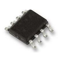
LM27222M National Semiconductor, LM27222M Datasheet - Page 4

LM27222M
Manufacturer Part Number
LM27222M
Description
MOSFET DRIVER/PWM CONTROL, 27222
Manufacturer
National Semiconductor
Datasheet
1.LM27222M.pdf
(11 pages)
Specifications of LM27222M
Device Type
MOSFET
Module Configuration
High Side / Low Side
Peak Output Current
4.5A
Output Resistance
10kohm
Supply Voltage Range
4V To 7V
Driver Case Style
SOIC
No. Of Pins
8
Operating
RoHS Compliant
Available stocks
Company
Part Number
Manufacturer
Quantity
Price
Part Number:
LM27222MX
Manufacturer:
NS/国半
Quantity:
20 000
www.national.com
POWER SUPPLY
HIGH-SIDE DRIVER
LOW-SIDE DRIVER
PULL-DOWN RESISTANCES
LEAKAGE CURRENTS
Absolute Maximum Ratings
If Military/Aerospace specified devices are required,
please contact the National Semiconductor Sales Office/
Distributors for availability and specifications.
Electrical Characteristics
VCC = CB = 5V, SW = GND = 0V, unless otherwise specified. Typicals and limits appearing in plain type apply for T
+25˚C. Limits appearing in boldface type apply over the entire operating temperature range (-40˚C ≤ T
Symbol
V
CB to GND
CB to SW
SW to GND (Note 2)
LEN to GND
IN to GND
LG to GND
HG to GND
t
I
R
R
on_min
R
R
leak_IN
I
CC
q_op
H-pu
H-pd
L-pu
L-pd
t
t
t
t
t
t
t
t
4
6
3
5
8
2
7
1
to GND
Operating Quiescent Current
Peak Pull-up Current
Pull-up Rds_on
Peak Pull-down Current
Pull-down Rds_on
Rise Time
Fall Time
Pull-up Dead Time
Pull-down Delay
Minimum Positive Output
Pulse Width
Peak Pull-up Current
Pull-up Rds_on
Peak Pull-down Current
Pull-down Rds_on
Rise Time
Fall Time
Pull-up Dead Time
Pull-down Delay
HG-SW Pull-down Resistance
LG-GND Pull-down
Resistance
LEN-GND Pull-down
Resistance
IN-GND Pull-down Resistance
IN pin Leakage Current
Parameter
(Note 4)
IN = 0V, LEN = 0V
IN = 0V, LEN = 5V
I
I
Timing Diagram, C
Timing Diagram, C
Timing Diagram
Timing Diagram
I
I
Timing Diagram, C
Timing Diagram, C
Timing Diagram
Timing Diagram
IN = 0V, Source Current
IN = 5V, Sink Current
CB
SW
VCC
GND
-0.3V to 36V
-0.2V to 36V
-0.3V to 36V
= I
(Note 1)
-0.3V to 7V
-0.3V to 7V
-0.3V to 7V
-0.3V to 7V
-0.3V to 7V
= I
= I
= I
HG
HG
LG
LG
= 0.3A
= 0.3A
= 0.3A
= 0.3A
Conditions
LOAD
LOAD
LOAD
LOAD
4
Operating Ratings
= 3.3nF
= 3.3nF
= 3.3nF
= 3.3nF
Junction Temperature
Power Dissipation (Note 3)
Storage Temperature
ESD Susceptibility
VCC
Junction Temperature Range
CB (max)
Human Body Model
Min
500
150K
150K
16.5
11.5
Typ
540
10k
10k
0.9
4.5
0.4
9.5
3.2
0.9
4.5
0.4
7.7
17
12
30
17
14
50
33
5
3
(Note 1)
J
≤ 125˚C).
Max
650
825
2.5
1.5
2.5
1.5
15
30
−65˚ to 150˚C
−40˚ to 125˚C
4V to 7V
A
720mW
+150˚C
= T
Units
µA
µA
nA
µA
ns
ns
ns
ns
ns
ns
ns
ns
ns
Ω
Ω
Ω
Ω
Ω
A
A
A
A
Ω
Ω
Ω
2kV
33V
J
=


