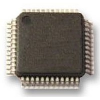
PCA9626B NXP Semiconductors, PCA9626B Datasheet - Page 8

PCA9626B
Manufacturer Part Number
PCA9626B
Description
IC, LED DRIVER, RGBA, 48-LQFP
Manufacturer
NXP Semiconductors
Datasheet
1.PCA9626B118.pdf
(47 pages)
Specifications of PCA9626B
No. Of Outputs
24
Output Current
100mA
Output Voltage
40V
Input Voltage
2.3V To 5.5V
Dimming Control Type
PWM
Driver Case Style
LQFP
Switching Frequency
1MHz
Base Number
9626
Operating
RoHS Compliant
Led Driver Application
RGB Or RGBA LED Drivers, LED Status Information, Displays, Backlights
Rohs Compliant
Yes
Lead Free Status / Rohs Status
Details
Available stocks
Company
Part Number
Manufacturer
Quantity
Price
Part Number:
PCA9626B
Manufacturer:
NXP/恩智浦
Quantity:
20 000
Company:
Part Number:
PCA9626B,118
Manufacturer:
NXP Semiconductors
Quantity:
10 000
Part Number:
PCA9626B,118
Manufacturer:
NXP/恩智浦
Quantity:
20 000
Company:
Part Number:
PCA9626B/S911
Manufacturer:
FREESCALE
Quantity:
430
Part Number:
PCA9626BS
Manufacturer:
NXP/恩智浦
Quantity:
20 000
Company:
Part Number:
PCA9626BЈ¬118
Manufacturer:
PH3
Quantity:
90
NXP Semiconductors
PCA9626_2
Product data sheet
7.1.2 LED All Call I
7.1.3 LED Sub Call I
7.1.4 Software Reset I
The last bit of the address byte defines the operation to be performed. When set to logic 1
a read is selected, while a logic 0 selects a write operation.
See
Remark: The default LED All Call I
as a regular I
PCA9626s on the I
See
Remark: The default LED Sub Call I
slave addresses as long as they are disabled.
The address shown in
performed by the master. The Software Reset address (SWRST Call) must be used with
R/W = logic 0. If R/W = logic 1, the PCA9626 does not acknowledge the SWRST. See
Section 7.6 “Software reset”
Remark: The Software Reset I
as a regular I
Fig 5.
•
•
•
•
•
•
•
Default power-up value (ALLCALLADR register): E0h or 1110 000
Programmable through I
At power-up, LED All Call I
E0h (R/W = 0) or E1h (R/W = 1) is sent by the master.
3 different I
Default power-up values:
– SUBADR1 register: E2h or 1110 001
– SUBADR2 register: E4h or 1110 010
– SUBADR3 register: E8h or 1110 100
Programmable through I
At power-up, Sub Call I
ACK when E2h (R/W = 0) or E3h (R/W = 1), E4h (R/W = 0) or E5h (R/W = 1), or
E8h (R/W = 0) or E9h (R/W = 1) is sent by the master.
Section 7.3.9 “ALLCALLADR, LED All Call I
Section 7.3.8 “SUBADR1 to SUBADR3, I
Software Reset address
2
2
C-bus slave address since this address is enabled at power-up. All of the
C-bus slave address or as an LED All Call or LED Sub Call address.
2
2
C-bus addresses can be used
C-bus address
2
C-bus addresses
2
2
C-bus will acknowledge the address if sent by the I
C-bus address
Rev. 02 — 31 August 2009
Figure 5
2
C-bus addresses are disabled. PCA9626 does not send an
2
2
for more detail.
C-bus (volatile programming)
C-bus (volatile programming)
2
0
2
C-bus address is enabled. PCA9626 sends an ACK when
is used when a reset of the PCA9626 needs to be
C-bus address is a reserved address and cannot be used
0
2
C-bus address (E0h or 1110 000) must not be used
2
C-bus addresses may be used as regular I
0
0
24-bit Fm+ I
2
0
C-bus subaddress 1 to 3”
2
C-bus address”
1
002aab416
1
2
R/W
C-bus 100 mA 40 V LED driver
0
for more detail.
PCA9626
2
© NXP B.V. 2009. All rights reserved.
C-bus master.
for more detail.
2
C-bus
8 of 47


