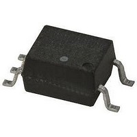
DS90LV012ATMF National Semiconductor, DS90LV012ATMF Datasheet - Page 4

DS90LV012ATMF
Manufacturer Part Number
DS90LV012ATMF
Description
IC, LVDS DIFF LINE RECEIVER, SOT-23-5
Manufacturer
National Semiconductor
Datasheet
1.DS90LT012ATMFNOPB.pdf
(8 pages)
Specifications of DS90LV012ATMF
Supply Current
9mA
Supply Voltage Range
2.7V To 3.6V
Driver Case Style
SOT-23
No. Of Pins
5
Operating Temperature Range
-40°C To +85°C
Device Type
Differential Line Receiver
Data Rate Max
400Mbps
Rohs Compliant
No
Lead Free Status / RoHS Status
Contains lead / RoHS non-compliant
Available stocks
Company
Part Number
Manufacturer
Quantity
Price
Part Number:
DS90LV012ATMF
Manufacturer:
NS/国半
Quantity:
20 000
Company:
Part Number:
DS90LV012ATMF/NOPB
Manufacturer:
ST
Quantity:
1 001
Part Number:
DS90LV012ATMF/NOPB
Manufacturer:
NS/国半
Quantity:
20 000
Company:
Part Number:
DS90LV012ATMFX
Manufacturer:
RENESAS
Quantity:
11 000
Part Number:
DS90LV012ATMFX
Manufacturer:
TI/德州仪器
Quantity:
20 000
Company:
Part Number:
DS90LV012ATMFX/NOPB
Manufacturer:
YAGEO
Quantity:
460 000
www.national.com
Typical Applications
Applications Information
General application guidelines and hints for LVDS drivers and
receivers may be found in the following application notes:
LVDS Owner's Manual (lit #550062-002), AN-808, AN-977,
AN-971, AN-916, AN-805, AN-903.
LVDS drivers and receivers are intended to be primarily used
in an uncomplicated point-to-point configuration as is shown
in Figure 3. This configuration provides a clean signaling en-
vironment for the fast edge rates of the drivers. The receiver
is connected to the driver through a balanced media which
may be a standard twisted pair cable, a parallel pair cable, or
simply PCB traces. Typically the characteristic impedance of
the media is in the range of 100Ω. A termination resistor of
100Ω should be selected to match the media, and is located
as close to the receiver input pins as possible. The termination
resistor converts the driver output (current mode) into a volt-
age that is detected by the receiver. Other configurations are
possible such as a multi-receiver configuration, but the effects
of a mid-stream connector(s), cable stub(s), and other
impedance discontinuities as well as ground shifting, noise
margin limits, and total termination loading must be taken into
account.
FIGURE 2. Receiver Propagation Delay and Transition Time Waveforms
FIGURE 3. Point-to-Point Application (DS90LV012A)
FIGURE 4. Point-to-Point Application (DS90LT012A)
Balanced System
Balanced System
4
The DS90LV012A and DS90LT012A differential line re-
ceivers are capable of detecting signals as low as 100 mV,
over a ±1V common-mode range centered around +1.2V.
This is related to the driver offset voltage which is typically
+1.2V. The driven signal is centered around this voltage and
may shift ±1V around this center point. The ±1V shifting may
be the result of a ground potential difference between the
driver's ground reference and the receiver's ground refer-
ence, the common-mode effects of coupled noise, or a com-
bination of the two. The AC parameters of both receiver input
pins are optimized for a recommended operating input volt-
age range of 0V to +2.4V (measured from each pin to ground).
The device will operate for receiver input voltages up to V
but exceeding V
which will clamp the bus voltages.
POWER DECOUPLING RECOMMENDATIONS
Bypass capacitors must be used on power pins. Use high fre-
quency ceramic (surface mount is recommended) 0.1μF and
0.001μF capacitors in parallel at the power supply pin with the
smallest value capacitor closest to the device supply pin. Ad-
ditional scattered capacitors over the printed circuit board will
improve decoupling. Multiple vias should be used to connect
DD
will turn on the ESD protection circuitry
20015005
20015028
20015004
DD
,


