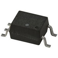
DS90LV012ATMF National Semiconductor, DS90LV012ATMF Datasheet - Page 2

DS90LV012ATMF
Manufacturer Part Number
DS90LV012ATMF
Description
IC, LVDS DIFF LINE RECEIVER, SOT-23-5
Manufacturer
National Semiconductor
Datasheet
1.DS90LT012ATMFNOPB.pdf
(8 pages)
Specifications of DS90LV012ATMF
Supply Current
9mA
Supply Voltage Range
2.7V To 3.6V
Driver Case Style
SOT-23
No. Of Pins
5
Operating Temperature Range
-40°C To +85°C
Device Type
Differential Line Receiver
Data Rate Max
400Mbps
Rohs Compliant
No
Lead Free Status / RoHS Status
Contains lead / RoHS non-compliant
Available stocks
Company
Part Number
Manufacturer
Quantity
Price
Part Number:
DS90LV012ATMF
Manufacturer:
NS/国半
Quantity:
20 000
Company:
Part Number:
DS90LV012ATMF/NOPB
Manufacturer:
ST
Quantity:
1 001
Part Number:
DS90LV012ATMF/NOPB
Manufacturer:
NS/国半
Quantity:
20 000
Company:
Part Number:
DS90LV012ATMFX
Manufacturer:
RENESAS
Quantity:
11 000
Part Number:
DS90LV012ATMFX
Manufacturer:
TI/德州仪器
Quantity:
20 000
Company:
Part Number:
DS90LV012ATMFX/NOPB
Manufacturer:
YAGEO
Quantity:
460 000
www.national.com
V
V
V
I
ΔI
I
R
C
V
V
I
V
I
Symbol
IN
IND
OS
DD
TH
TL
CM
OH
OL
CL
T
IN
IN
Absolute Maximum Ratings
If Military/Aerospace specified devices are required,
please contact the National Semiconductor Sales Office/
Distributors for availability and specifications.
Electrical Characteristics
Over Supply Voltage and Operating Temperature ranges, unless otherwise specified. (Notes 2, 3)
Supply Voltage (V
Input Voltage (IN+, IN−)
Output Voltage (TTL OUT)
Output Short Circuit Current
Maximum Package Power Dissipation @ +25°C
LDA Package
Derate LDA Package
Thermal resistance (θ
MF Package
Derate MF Package
Differential Input High Threshold
Differential Input Low Threshold
Common-Mode Voltage
Input Current (DS90LV012A)
Change in Magnitude of I
Differential Input Current
(DS90LT012A)
Integrated Termination Resistor
(DS90LT012A)
Input Capacitance
Output High Voltage
Output Low Voltage
Output Short Circuit Current
Input Clamp Voltage
No Load Supply Current
DD
Parameter
)
JA
)
IN
18.1 mW/°C above +25°C
7.22 mW/°C above +25°C
−0.3V to (V
V
V
V
V
V
V
V
V
V
V
V
IN+ = IN− = GND
I
I
I
I
V
I
Inputs Open
OH
OH
OH
OL
CL
−0.3V to +3.9V
CM
DD
DD
IN
IN
IN
IN
IN
IN
IN+
IN+
OUT
−0.3V to +4V
= −18 mA
= 2 mA, V
= +2.8V
= 0V
= +3.6V
= +2.8V
= 0V
= +3.6V
= −0.4 mA, V
= −0.4 mA, Inputs terminated
= −0.4 mA, Inputs shorted
(Note 1)
= 2.7V, V
= 3.0V to 3.6V, V
dependant on V
= +0.4V, V
= +2.4V, V
= 0V (Note 5)
DD
55.3°C/W
−100mA
902mW
+ 0.3V)
2.26 W
Conditions
ID
ID
V
V
V
V
IN−
IN−
= −200 mV
= 100mV
DD
DD
DD
DD
ID
= +0V
= +2.0V
= +200 mV
= 3.6V or 0V
= 0V
= 3.6V or 0V
= 0V
2
DD
ID
(Note 11)
= 100mV
Recommended Operating
Conditions
Storage Temperature Range
Lead Temperature Range Soldering
Maximum Junction Temperature
ESD Ratings (Note 4)
Supply Voltage (V
Operating Free Air
Thermal resistance (θ
(4 sec.)
Temperature (T
TTL OUT
IN+, IN−
V
Pin
DD
A
DD
)
)
JA
−100
−1.5
0.05
0.05
Min
−10
−10
−20
−15
)
2.4
2.4
2.4
3
+2.7
Min
−40
−0.7
Typ
−30
−30
102
−50
3.9
3.1
3.1
3.1
0.3
5.4
±1
±1
4
4
4
3
+3.3
Typ
25
−65°C to +150°C
V
DD
+3.6
Max
−100
+85
Max
2.35
+10
+10
+20
4.4
0.5
- 0.3V
0
9
138.5°C/W
+260°C
+150°C
Units
°C
V
Units
mV
mV
mA
mA
mA
μA
μA
μA
μA
μA
μA
pF
V
V
Ω
V
V
V
V
V


