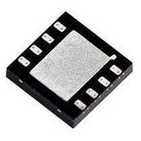
DS90LV001TLD National Semiconductor, DS90LV001TLD Datasheet - Page 2

DS90LV001TLD
Manufacturer Part Number
DS90LV001TLD
Description
IC, LVDS BUFFER, LLP-8
Manufacturer
National Semiconductor
Datasheet
1.DS90LV001TLD.pdf
(16 pages)
Specifications of DS90LV001TLD
Supply Current
70mA
Supply Voltage Range
3V To 3.6V
Driver Case Style
LLP
No. Of Pins
8
Operating Temperature Range
-40°C To +85°C
Termination Type
SMD
Logic Type
Buffer
Transceiver Type
Buffer
Filter Terminals
SMD
Rohs Compliant
No
Data Rate
800Mbps
Data Rate Max
800Mbps
Family Type
LV
Lead Free Status / RoHS Status
Contains lead / RoHS non-compliant
Available stocks
Company
Part Number
Manufacturer
Quantity
Price
Company:
Part Number:
DS90LV001TLD/NOPB
Manufacturer:
NS
Quantity:
8 746
Company:
Part Number:
DS90LV001TLDX/NOPB
Manufacturer:
NS
Quantity:
8 597
www.national.com
LVCMOS/LVTTL DC SPECIFICATIONS (EN)
V
V
I
I
V
LVDS OUTPUT DC SPECIFICATIONS (OUT)
V
ΔV
V
ΔV
I
I
I
I
LVDS RECEIVER DC SPECIFICATIONS (IN)
V
V
V
I
ΔI
SUPPLY CURRENT
I
I
Symbol
IH
IL
OZ
OFF
OS
OSD
IN
CCD
CCZ
Supply Voltage (V
LVCMOS/LVTTL Input Voltage
(EN)
LVDS Receiver Input Voltage (IN
+, IN−)
LVDS Driver Output Voltage (OUT
+, OUT−)
LVDS Output Short Circuit Current
Junction Temperature
Storage Temperature Range
Lead Temperature Range
IH
IL
CL
OD
OS
TH
TL
CMR
IN
Absolute Maximum Ratings
If Military/Aerospace specified devices are required,
please contact the National Semiconductor Sales Office/
Distributors for availability and specifications.
Electrical Characteristics
Over recommended operating supply and temperature ranges unless otherwise specified. (Notes 2, 3)
OD
OS
Soldering (4 sec.)
High Level Input Voltage
Low Level Input Voltage
High Level Input Current
Low Level Input Current
Input Clamp Voltage
Differential Output Voltage
Change in Magnitude of V
Output States
Offset Voltage
Change in Magnitude of V
Output States
Output TRI-STATE Current
Power-Off Leakage Current
Output Short Circuit Current (Note 4)
Differential Output Short Circuit Current (Note 4)
Differential Input High Threshold
Differential Input Low Threshold
Common Mode Voltage Range
Input Current
Change in Magnitude of I
Total Supply Current
TRI-STATE Supply Current
CC
)
Parameter
IN
OD
OS
for Complimentary
for Complimentary
−0.3V to (V
−65°C to +150°C
(Note 1)
−0.3V to +4V
−0.3V to +4V
−0.3V to +4V
Continuous
CC
+150°C
+260°C
+ 0.3V)
V
V
I
R
Figure 1 and Figure 2
R
Figure 1
EN = 0V, V
V
EN = V
EN = V
V
V
V
V
V
V
EN = V
EN = 0V
CL
IN
IN
L
L
CC
CM
ID
IN
IN
IN
IN
= 100Ω
= 100Ω
= −18 mA
= 3.6V or 2.0V, V
= GND or 0.8V, V
= 100mV, V
= +3.0V
= 0V
= +3.0V
= 0V
2
= 0V, V
= +0.05V, +1.2V or +3.25V
Maximum Package Power Dissipation at 25°C
ESD Ratings
CC
CC
CC
Recommended Operating
Conditions
Supply Voltage (V
Receiver Input Voltage
Operating Free Air
Temperature
M Package
Derate M Package
LDA Package
Derate LDA Package
(HBM, 1.5kΩ, 100pF)
(EIAJ, 0Ω, 200pF)
, V
, V
, R
OUT
OUT
OUT+
OD
Conditions
L
= 100Ω, C
= V
= 0V
CC
= 3.6V or GND
V
V
and V
CC
CC
= 3.3V
CC
= 3.6V or 0V
= 3.6V or 0V
CC
CC
or GND
OUT−
= 3.6V
= 3.6V
L
= 5 pF
CC
= 0V
)
Min
−40
3.0
1.080
GND
−100
0
0.05
Min
250
2.0
19.49 mW/°C above +25°C
5.8 mW/°C above +25°C
Typ
+25
3.3
−0.6
1.19
Typ
325
−16
+7
±1
±1
±1
−7
±1
±1
47
22
0
0
1
1
Max
V
+85
3.6
CC
1.375
+100
Max
−1.5
3.25
V
+20
±10
450
±10
±10
−24
−12
±10
±10
0.8
20
20
70
35
6
6
CC
Units
726 mW
≥
°C
2.44 W
≥
V
V
2.5kV
Units
250V
mV
mV
mV
mA
mA
mV
mV
mA
mA
μA
μA
μA
μA
μA
μA
μA
μA
V
V
V
V
V


