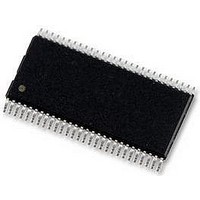
PCF8578T/1 NXP Semiconductors, PCF8578T/1 Datasheet - Page 29

PCF8578T/1
Manufacturer Part Number
PCF8578T/1
Description
IC, LCD DRIVER, ROW/COLUMN, 56VSOP
Manufacturer
NXP Semiconductors
Datasheet
1.PCF8578T1.pdf
(46 pages)
Specifications of PCF8578T/1
Supply Current
20µA
No. Of Digits / Alpha
36
Meter Display Type
LCD
Supply Voltage Range
2.5V To 6V
Driver Case Style
VSOP
No. Of Pins
56
Operating Temperature Range
-40°C To +85°C
Base
RoHS Compliant
No. Of Segments
384
Interface Type
I2C
Rohs Compliant
Yes
Available stocks
Company
Part Number
Manufacturer
Quantity
Price
Part Number:
PCF8578T/1
Manufacturer:
NXP/恩智浦
Quantity:
20 000
Part Number:
PCF8578T/1,118
Manufacturer:
NXP/恩智浦
Quantity:
20 000
NXP Semiconductors
10. Static characteristics
Table 17.
V
[1]
[2]
[3]
[4]
PCF8578_6
Product data sheet
Symbol
Supplies
V
V
I
V
Logic
V
V
I
I
I
C
LCD outputs
I
V
R
DD
OL
OH
L
L
DD
DD
LCD
POR
IL
IH
offset(DC)
i
O
= 2.5 V to 6 V; V
Outputs are open; inputs at V
Resets all logic when V
Periodically sampled; not 100 % tested.
Resistance measured between output terminal (R0 to R7, R8/C8 to R31/C31 and C32 to C39) and bias input (V
when the specified current flows through one output under the following conditions (see
a) V
b) Row mode, R0 to R7 and R8/C8 to R31/C31: V
c) Column mode, R8/C8 to R31/C31 and C32 to C39: V
oper
Static characteristics
= V
Parameter
supply voltage
LCD supply voltage
supply current
LOW-level input voltage
HIGH-level input voltage
LOW-level output current
HIGH-level output current
leakage current
capacitance for each I/O pin
leakage current
DC offset voltage
output resistance
power-on reset voltage
DD
V
SS
LCD
= 0 V; V
= 9 V.
DD
< V
DD
POR
LCD
or V
.
= V
SS
; I
DD
2
C-bus inactive; external clock with 50 % duty factor.
3.5 V to V
Conditions
external clock;
internal clock;
at pins SYNC and CLK;
V
at pin SDA;
V
at pins SYNC and CLK;
V
at pins SDA, SCL, SYNC,
CLK, TEST and SA0;
V
at pin OSC;
V
at pins V
V
on pins R0 to R7, R8/C8 to
R31/C31 and C32 to C39
on row output pins: R0 to
R7 and R8/C8 to R31/C31
on column output pins:
R8/C8 to R31/C31 and C32
to C39
2
OL
OL
OH
i
i
i
f
R
= V
= V
= V
clk
Rev. 06 — 5 May 2009
ext(OSC)
V
= 1 V; V
= 0.4 V; V
= 4 V; V
= 2 kHz
LCD
DD
DD
DD
DD
3
2
or V
or V
V
to V
6.65 V; V
LCD
9 V; T
LCD row/column driver for dot matrix graphic displays
= 330 k
DD
DD
SS
LCD
DD
5
;
= 5 V
= 5 V;
4.70 V; V
amb
= 5 V
5
= 40 C to +85 C; unless otherwise specified.
V
LCD
4
V
LCD
2.35 V; I
[1]
[2]
[3]
[4]
[4]
Min
2.5
V
-
-
0.8
V
0.7V
1
3
-
-
-
-
-
4.30 V; I
Table 6 on page
1
1
2
DD
SS
load
DD
= 150 A.
9
load
= 100 A.
Typ
-
-
6
20
1.3
-
-
-
-
-
-
-
-
-
1.5
3
20
11):
PCF8578
2
© NXP B.V. 2009. All rights reserved.
to V
Max
6.0
V
15
50
1.8
0.3V
V
-
-
+1
+1
5
+2
-
3
6
1
DD
DD
5
, V
DD
DD
3.5
and V
29 of 46
Unit
V
V
V
V
V
mA
mA
mA
mA
pF
mV
k
k
LCD
A
A
A
A
)


