EVAL-ADF7012DBZ4 Analog Devices Inc, EVAL-ADF7012DBZ4 Datasheet - Page 16
EVAL-ADF7012DBZ4
Manufacturer Part Number
EVAL-ADF7012DBZ4
Description
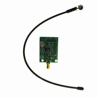
BOARD EVALUATION DB4 FOR ADF7012
Manufacturer
Analog Devices Inc
Type
Transmitterr
Datasheet
1.EVAL-ADF7012EB1.pdf
(28 pages)
Specifications of EVAL-ADF7012DBZ4
Frequency
1GHz
For Use With/related Products
ADF7012
Lead Free Status / RoHS Status
Lead free / RoHS Compliant


ADF7012
OUTPUT DIVIDER
An output divider is a programmable divider following the
VCO in the PLL loop. It is useful when using the ADF7012 to
generate frequencies of < 500 MHz.
The output divider may be used to reduce feedthrough of the
VCO by amplifying only the VCO/2 component, restricting the
VCO feedthrough to leakage.
Because the divider is in loop, the N register values should be
set up according to the usual formula. However, the VCO gain
(K
in the following example:
Therefore, K
The divider value is set in the R register.
Table 5.
OD1
0
0
1
1
MUXOUT MODES
The MUXOUT pin allows the user access to various internal
signals in the transmitter, and provides information on the
PLL lock status, the regulator, and the battery voltage. The
MUXOUT is accessed by programming Bits M1 to M4 in the
function register and observing the signal at the MUXOUT pin.
V
) should be scaled according to the divider setting, as shown
F
F
K
OUT
VCO
V
REFERENCE
DIVIDER
@ 868 MHz = 60 MHz/V
= 433 MHz
= 866 MHz
V
for loop filter design = 30 MHz/V.
Figure 35. Output Divider Location in PLL
PFD
OD2
0
1
0
1
CP
FILTER
LOOP
÷N
VCO
OUTPUT
DIVIDER
÷1/2/4/8
Divider Status
Divider off
Divide by 2
Divide by 4
Divide by 8
PA
Rev. A | Page 16 of 28
Battery Voltage Readback
By setting MUXOUT to 1010 to 1101, the battery voltage can
be estimated. The battery measuring circuit features a voltage
divider and a comparator where the divided-down supply
voltage is compared to the regulator voltage.
Table 6.
MUXOUT
1010
1011
1100
1101
The accuracy of the measurement is limited by the accuracy of
the regulator voltage and the internal resistor tolerances.
Regulator Ready
The regulator has a power-up time, dependant on process and
the external capacitor. The regulator ready signal indicates that
the regulator is fully powered, and that the serial interface is
active. This is the default setting on power-up at MUXOUT.
Digital Lock Detect
Digital lock detect indicates that the status of the PLL loop.
The PLL loop takes time to settle on power-up and when the
frequency of the loop is changed by changing the N value.
When lock detect is high, the PFD has counted a number of
consecutive cycles where the phase error is < 15 ns. The lock
detect precision bit in the function register determines whether
this is three cycles (LDP = 0), or five cycles (LDP = 1). It is
recommended that LDP be set to 1. The lock detect is not
completely accurate and goes high before the output has settled
to exactly the correct frequency. In general, add 50% to the
indicated lock time to obtain lock time to within 1 kHz. The
lock detect signal can be used to decide when the power
amplifier (PA) should be enabled.
R Divider
MUXOUT provides the output of the R divider. This is a
narrow pulsed digital signal at frequency F
may be used to check the operation of the crystal circuit and
the R divider. R divider/2 is a buffered version of this signal
at F
PFD
/2.
MUXOUT High
DV
DV
DV
DV
DD
DD
DD
DD
< 2.35 V
< 2.75 V
< 3.0 V
< 3.25 V
PFD
MUXOUT Low
DV
DV
DV
DV
. This signal
DD
DD
DD
DD
> 2.35 V
> 2.75 V
> 3.0 V
> 3.25 V
Related parts for EVAL-ADF7012DBZ4
Image
Part Number
Description
Manufacturer
Datasheet
Request
R

Part Number:
Description:
IC, ADJ LDO REG, 1.5V TO 5V 250mA MSOP-8
Manufacturer:
Vishay
Datasheet:

Part Number:
Description:
IC, ADJ LDO REG, 1.5V TO 5V 0.6A 8-TSSOP
Manufacturer:
Vishay
Datasheet:
Part Number:
Description:
IC, ADJ LDO REG, 1.5V TO 5V 250mA MSOP-8
Manufacturer:
Vishay
Datasheet:

Part Number:
Description:
IC ADJ LDO REG 1.5V TO 5V 150mA 5-SOT-23
Manufacturer:
Vishay
Datasheet:

Part Number:
Description:
BOARD EVAL AS1324-AD
Manufacturer:
austriamicrosystems
Datasheet:
Part Number:
Description:
IC, ADJ LDO REG, 1.5V TO 5V 0.6A 8-TSSOP
Manufacturer:
Vishay
Datasheet:

Part Number:
Description:
IC, ADJ LDO REG, 1.5V TO 5V, 0.3A, MSOP8
Manufacturer:
Vishay
Datasheet:
Part Number:
Description:
IC, ADJ LDO REG, 1.5V TO 5V, 0.3A, MSOP8
Manufacturer:
Vishay
Datasheet:
Part Number:
Description:
IC, ADJ LDO REG 1.215V TO 5V 0.3A MSOP-8
Manufacturer:
Vishay
Datasheet:
Part Number:
Description:
IC, ADJ LDO REG 1.215V TO 5V 0.3A MSOP-8
Manufacturer:
Vishay
Datasheet:

Part Number:
Description:
±1.7g Dual-Axis IMEMS Accelerometer Evaluation Board
Manufacturer:
Analog Devices Inc
Datasheet:

Part Number:
Description:
IC MULTIPLIER ANALOG 8-SOIC T/R
Manufacturer:
Analog Devices Inc
Datasheet:

Part Number:
Description:
IC ANALOG MULTIPLIER 8-DIP
Manufacturer:
Analog Devices Inc
Datasheet:
Part Number:
Description:
IC ANALOG MULTIPLIER 8-SOIC
Manufacturer:
Analog Devices Inc
Datasheet:
Part Number:
Description:
IC ANALOG MULTIPLIER 8-DIP
Manufacturer:
Analog Devices Inc
Datasheet: