EVALSF3-ICE3B1565 Infineon Technologies, EVALSF3-ICE3B1565 Datasheet - Page 7
EVALSF3-ICE3B1565
Manufacturer Part Number
EVALSF3-ICE3B1565
Description
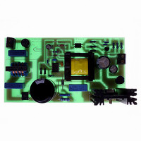
BOARD DEMO ICE3B1565 20W SMPS
Manufacturer
Infineon Technologies
Series
CoolSET®F3r
Datasheet
1.EVALSF3-ICE3B1565.pdf
(16 pages)
Specifications of EVALSF3-ICE3B1565
Main Purpose
AC/DC, Primary Side
Outputs And Type
1, Isolated
Power - Output
20W
Voltage - Output
16V
Current - Output
1.25A
Voltage - Input
85 ~ 265VAC
Regulator Topology
Flyback
Frequency - Switching
67kHz
Board Type
Fully Populated
Utilized Ic / Part
ICE3B1565
Lead Free Status / RoHS Status
Lead free / RoHS Compliant
Other names
EVALSF3-ICE3B1565IN


4
4.1
The AC line input side comprises the input fuse F1 as over-current protection. The choke L1, X2-capacitors
C1, C2 and Y1-capacitor C5 act as radio interference suppressors. After the bridge rectifier BR1 and the
input capacitor C3, a voltage of 80 to 380 VDC depending on input voltage is available.
4.2
The PWM pulse is generated by 8-pin CoolSET™F3 ICE3B1565. ICE3B1565 is an integrated power IC
which includes both of the current- mode PWM controller and a CoolMOS
The control IC and CoolMOS
no compromise like monolithic approaches is necessary.
4.3
R1, C4 and D1 dissipate the energy of the leakage inductance.
4.4
The primary current is sensed by the external shunt resistor R4 and R4A. The sense voltage is fed into
ICE3B1565 and a cycle by cycle current limiting is achieved. Primary current is being converted to a
corresponding voltage level at CS pin. A 220ns leading edge blanking is provided to avoid leading edge
spikes from distorting the current limiting.
4.5
On the secondary side the power is coupled out by an ultra-fast diode BYW29E150. The capacitor C13,
provide energy buffering following with the LC filter, L2 and C12 to reduce the output voltage ripple
considerably. Storage capacitor C13 is selected to have an internal resistance as small as possible (ESR) to
minimizes the output voltage ripple
4.6
The output voltage is sensed by the voltage divider of R8, R9 and R10 and compare to TL431 internal
reference voltage. The output voltage of TL431, IC3 is transferred to the primary via an optocoupler, IC2 for
regulation control. The secondary regulation control is adopted with TL431 and optocoupler. C10, C11, R7
being the compensation network constitutes the external circuitry of the error amplifier of TL431. This
circuitry allows the feedback to be precisely matched to dynamically varying load conditions, thereby
providing stable control. The maximum current through the optocoupler diode and the voltage reference is
limited by the resistor R5 and R6. Optocoupler IC2 is used for floating transmission of the control signal to
the “FB” input of the ICE3B1565.
4.7
In case of Load Jumps the Controller provides a Blanking Window before activating the Overvoltage
Protection and entering the Auto Restart Mode. This time is generated by charging up the Soft Start
capacitor from 4.4V to 5.4V. Within this timeframe the voltage at Feedback pin can rise up above 4.8V,
without switching off due to Overload Protection. During this operation the transferred power is limited to the
maximum peak current defined by the value of the sense resistor. The same procedure happens to the
Application Note
Circuit Description
Line Input
PWM Control and Power Stage
Clamping Network
Primary Current Sense
Output Stage
Feedback Loop
Blanking Window for Load Jump / Active Burst Mode
TM
are fabricated by the different optimized chip technologies respectively and
7
TM
with 650V breakdown voltage.
ICE3B1565
2005-01-13
Related parts for EVALSF3-ICE3B1565
Image
Part Number
Description
Manufacturer
Datasheet
Request
R

Part Number:
Description:
BOARD DEMO ICE3DS01G 60W SO-8
Manufacturer:
Infineon Technologies
Datasheet:

Part Number:
Description:
BOARD DEMO ICE3A5565P 100W SMPS
Manufacturer:
Infineon Technologies
Datasheet:

Part Number:
Description:
BOARD DEMO ICE3B2065P 40W SMPS
Manufacturer:
Infineon Technologies
Datasheet:

Part Number:
Description:
BOARD DEMO ICE3B0565 15W SMPS
Manufacturer:
Infineon Technologies
Datasheet:

Part Number:
Description:
BOARD DEMO ICE3B2565 30.4W SMPS
Manufacturer:
Infineon Technologies
Datasheet:

Part Number:
Description:
BOARD DEMO ICE3DS01 60W 8-DIP
Manufacturer:
Infineon Technologies
Datasheet:

Part Number:
Description:
Manufacturer:
Infineon Technologies AG
Datasheet:
Part Number:
Description:
Manufacturer:
Infineon Technologies AG
Datasheet:
Part Number:
Description:
Manufacturer:
Infineon Technologies AG
Datasheet:
Part Number:
Description:
Manufacturer:
Infineon Technologies AG
Datasheet:
Part Number:
Description:
Manufacturer:
Infineon Technologies AG
Datasheet:
Part Number:
Description:
Manufacturer:
Infineon Technologies AG
Datasheet:
Part Number:
Description:
Manufacturer:
Infineon Technologies AG
Datasheet:
Part Number:
Description:
16-bit microcontroller with 2x2 KByte RAM
Manufacturer:
Infineon Technologies AG
Datasheet:
Part Number:
Description:
NPN silicon RF transistor
Manufacturer:
Infineon Technologies AG
Datasheet: