EVL90WADP-LLCSR STMicroelectronics, EVL90WADP-LLCSR Datasheet - Page 7
EVL90WADP-LLCSR
Manufacturer Part Number
EVL90WADP-LLCSR
Description
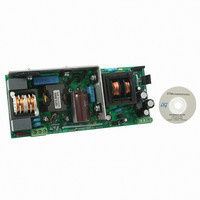
EVAL BOARD PORTABLE PWR SUPPLY
Manufacturer
STMicroelectronics
Type
Power Factor Correctionr
Datasheets
1.L6563HTR.pdf
(49 pages)
2.L6599ADTR.pdf
(36 pages)
3.EVL90WADP-LLCSR.pdf
(29 pages)
4.EVL90WADP-LLCSR.pdf
(28 pages)
Specifications of EVL90WADP-LLCSR
Main Purpose
AC/DC, Primary and Secondary Side with PFC
Outputs And Type
1, Isolated
Power - Output
90W
Voltage - Output
19V
Current - Output
4.75A
Voltage - Input
90 ~ 264VAC
Regulator Topology
Boost
Frequency - Switching
130kHz
Board Type
Fully Populated
Utilized Ic / Part
L6563H, L6599A, SRK2000
Input Voltage
90 V to 264 V
Output Voltage
19 V
Dimensions
65 mm x 155 mm
Product
Power Management Modules
Supply Current
4.75 A
Lead Free Status / RoHS Status
Lead free / RoHS Compliant
For Use With/related Products
L6563H, L6599A, SRK2000
Other names
497-10377


L6599A
Table 2.
Pin N#
10
11
12
13
14
15
16
9
PFC_STOP
Pin description (continued)
VBOOT
Type
GND
OUT
HVG
N.C.
LVG
Vcc
Open-drain ON/OFF control of PFC controller. This pin, normally open, is
intended for stopping the PFC controller, for protection purpose or during
burst-mode operation. It goes low when the IC is shut down by DIS>1.85 V,
ISEN > 1.5 V, LINE > 6 V and STBY < 1.24 V. The pin is pulled low also
when the voltage on pin DELAY exceeds 2 V and goes back open as the
voltage falls below 0.3 V. During UVLO, it is open. Leave the pin
unconnected if not used.
Chip ground. Current return for both the low-side gate-drive current and
the bias current of the IC. All of the ground connections of the bias
components should be tied to a track going to this pin and kept separate
from any pulsed current return.
Low-side gate-drive output. The driver is capable of 0.3 A min. source and
0.8 A min. sink peak current to drive the lower MOSFET of the half-bridge
leg. The pin is actively pulled to GND during UVLO.
Supply voltage of both the signal part of the IC and the low-side gate
driver. Sometimes a small bypass capacitor (0.1 µF typ.) to GND might be
useful to get a clean bias voltage for the signal part of the IC.
High-voltage spacer. The pin is not internally connected to isolate the high-
voltage pin and ease compliance with safety regulations (creepage
distance) on the PCB.
High-side gate-drive floating ground. Current return for the high-side gate-
drive current. Layout carefully the connection of this pin to avoid too large
spikes below ground.
High-side floating gate-drive output. The driver is capable of 0.3 A min.
source and 0.8 A min. sink peak current to drive the upper MOSFET of the
half-bridge leg. A resistor internally connected to pin 14 (OUT) ensures
that the pin is not floating during UVLO.
High-side gate-drive floating supply Voltage. The bootstrap capacitor
connected between this pin and pin 14 (OUT) is fed by an internal
synchronous bootstrap diode driven in-phase with the low-side gate-drive.
This patented structure replaces the normally used external diode.
Doc ID 15308 Rev 5
Function
Pin connection
7/36
Related parts for EVL90WADP-LLCSR
Image
Part Number
Description
Manufacturer
Datasheet
Request
R

Part Number:
Description:
STMicroelectronics [RIPPLE-CARRY BINARY COUNTER/DIVIDERS]
Manufacturer:
STMicroelectronics
Datasheet:
Part Number:
Description:
STMicroelectronics [LIQUID-CRYSTAL DISPLAY DRIVERS]
Manufacturer:
STMicroelectronics
Datasheet:

Part Number:
Description:
BOARD EVAL FOR MEMS SENSORS
Manufacturer:
STMicroelectronics
Datasheet:
Part Number:
Description:
NPN TRANSISTOR POWER MODULE
Manufacturer:
STMicroelectronics
Datasheet:
Part Number:
Description:
TURBOSWITCH ULTRA-FAST HIGH VOLTAGE DIODE
Manufacturer:
STMicroelectronics
Datasheet:
Part Number:
Description:
Manufacturer:
STMicroelectronics
Datasheet:
Part Number:
Description:
DIODE / SCR MODULE
Manufacturer:
STMicroelectronics
Datasheet:
Part Number:
Description:
DIODE / SCR MODULE
Manufacturer:
STMicroelectronics
Datasheet:
Part Number:
Description:
Search -----> STE16N100
Manufacturer:
STMicroelectronics
Datasheet:
Part Number:
Description:
Search ---> STE53NA50
Manufacturer:
STMicroelectronics
Datasheet:
Part Number:
Description:
NPN Transistor Power Module
Manufacturer:
STMicroelectronics
Datasheet:
Part Number:
Description:
DIODE / SCR MODULE
Manufacturer:
STMicroelectronics
Datasheet: