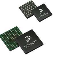
MC13892JVL Freescale Semiconductor, MC13892JVL Datasheet - Page 117

MC13892JVL
Manufacturer Part Number
MC13892JVL
Description
IC PMU I.MX51/37/35/27 186MAPBGA
Manufacturer
Freescale Semiconductor
Datasheets
1.MC13892AJVLR2.pdf
(156 pages)
2.MC13892AJVLR2.pdf
(2 pages)
3.MC13892AJVLR2.pdf
(16 pages)
4.MC13892JVL.pdf
(161 pages)
Specifications of MC13892JVL
Applications
Battery Management, Display (LED Drivers), Handheld/Mobile Devices, Power Supply
Operating Temperature
-40°C ~ 85°C
Mounting Type
Surface Mount
Package / Case
186-LFBGA
Output Current
65 mA
Output Voltage
1.5 V
Operating Temperature (max)
85C
Operating Temperature (min)
-40C
Mounting
Surface Mount
Package Type
BGA
Case Length
12mm
Screening Level
Industrial
Lead Free Status / RoHS Status
Lead free / RoHS Compliant
Current - Supply
-
Voltage - Supply
-
Lead Free Status / Rohs Status
Lead free / RoHS Compliant
Available stocks
Company
Part Number
Manufacturer
Quantity
Price
Company:
Part Number:
MC13892JVL
Manufacturer:
DALSA
Quantity:
4
Company:
Part Number:
MC13892JVL
Manufacturer:
Freescale Semiconductor
Quantity:
10 000
Part Number:
MC13892JVL
Manufacturer:
FREESCALE
Quantity:
20 000
Company:
Part Number:
MC13892JVLR2
Manufacturer:
Freescale Semiconductor
Quantity:
10 000
the enable for the boost converter is an OR of the following SPI bits (SWBSTEN, USBSWBSTEN, and LEDSWBSTEN). For more
details on the boost switcher and its control, see Supplies.
hardware. Ramp patterns for each of the drivers is accessed with the corresponding LEDxRAMP bit.
time is therefore a function of the initial set PWM cycle and the final PWM cycle. As an example, starting from 0/32 and going to
32/32 will take 500 ms while going to from 8/32 to 16/32 takes 125 ms.
when LEDxRAMP = 0, then the change is immediate rather than spread out over a PWM sweep.
that the intensity is set through the PWM duty cycle.
drivers through LEDxPER[1:0], while the on period is determined by the duty cycle setting. To avoid high frequency spur coupling
in the application, the switching edges of the output drivers are softened. During blinking, so LEDxPER[1:0] is not "00", ramping
and dimming patterns cannot be applied.
signaling or as generic PWM generator outputs. For the maximum voltage ratings.
Analog Integrated Circuit Device Data
Freescale Semiconductor
As with the backlight driver channels, the signaling LED drivers include ramp up and ramp down patterns are implemented in
The ramp itself is generated by increasing or decreasing the PWM duty cycle with a 1/32 step every 1/64 seconds. The ramp
Note that the ramp function is executed upon every change in PWM cycle setting. If a PWM change is programmed via SPI
For color mixing and in order to guarantee a constant color, the color mixing should be obtained by the current level setting so
In addition, programmable blink rates are provided. Blinking is obtained by lowering the PWM repetition rate of each of the
Apart from using the signal LED drivers for driving LEDs they can also be used as general purpose open drain outputs for logic
Table 110. Signaling LED Driver Characteristics
Absolute Accuracy
Matching
Leakage
Parameter
Table 109. Signal LED Drivers Period Control
LEDxPER[1:0]
At 400 mV, 21 mA
LEDxDC[5:0] = 000000
00
01
10
11
Condition
Repetition Rate
1/256
1/8
1
2
Min
-
-
-
Units
Typ
-
-
-
s
s
s
s
Max
FUNCTIONAL DEVICE OPERATION
1.0
15
10
Units
μ
%
%
A
LIGHTING SYSTEM
13892
117


